2-16
Theory
of
Operation
I
CHIP
SELECTS
I
,8
MEMORY
ADDRESS
BUS
,
,8
I
..
• •
.~
16K
X 8
~,
r+
16K
x 8
~
---+-
RAM
RAM
... ...
t t
~
16K
X 8
~
u-+
16K
X 8
~~
.~
RAM
RAM
.. ..
t
•
.~
16K
X 8
~~
.~
16K
X 8
f+-4~
~
RAM
RAM
--
...
I t
.......
16K
X 8
+-
4~
16K
X 8
~
4
.......
RAM
RAM
TO
MPB
j
32
I
,
MEMORY
CONTROLLER
JEMOty
tAT!
BJS
I
I
8 I
I
,8
,8
, ,
I
.-
.-
t t
16K
X 8
~
r+
16K
x 8
RAM
RAM
... ...
• •
16K
X 8
~~
~
16K
X 8
RAM
RAM
..
..
• •
16K
X 8
f+-4
0-+
16K
X 8
RAM RAM
...
...
t t
16K
X 8
~
0-+
16K
X 8
RAM
RAM
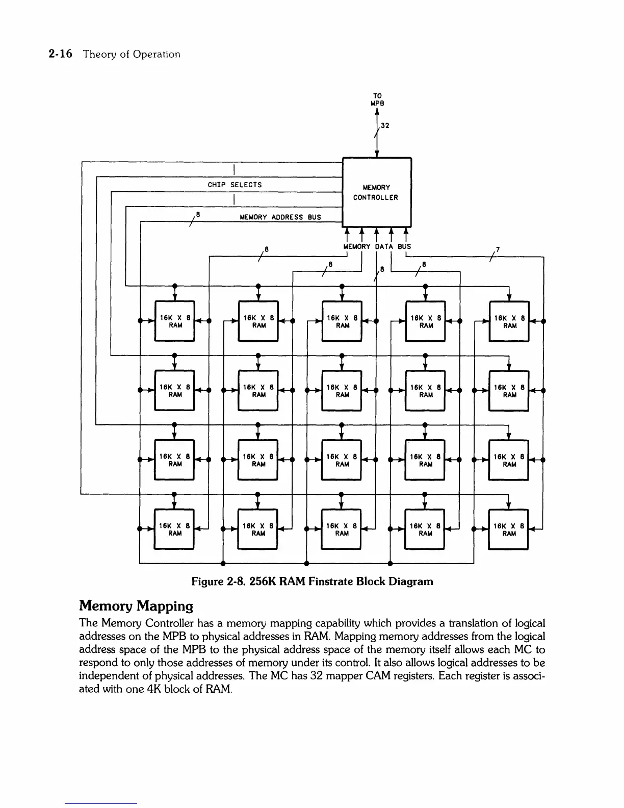
Figure 2-8. 256K
RAM
Finstrate Block Diagram
Memory Mapping
,7
,
t
~
r+
16K
x 8
~~
RAM
t
~
~
4
~
16K
X 8
f+-4'
RAM
+
~
H-+
16K
X 8
~.
RAM
t
.........
~
16K
X 8
+-
RAM
The Memory Controller has a memory mapping capability which provides a translation of logical
addresses
on
the
MPB
to physical addresses
in
RAM.
Mapping memory addresses from the logical
address space of the
MPB
to the physical address space of the memory itself allows each
MC
to
respond to only those addresses of memory under
its
control. It also allows logical addresses to
be
independent of physical addresses. The
MC
has
32
mapper
CAM
registers. Each register
is
associ-
ated with
one
4K block of
RAM.