IOPBUS
J4
(50-PIN)
POWER
J2
(50-PIN)
INTERFACE
BUFFERS
DATA
ALPHA
DATA
BUFFER
DIR G
FRAME BUFFER
ADDRESS WE
OE
S1
~
MTST ERR
CONTROLLER
CONTROL
DATA
LINE BUFFER
TST LD
Figure 2-20. Display Interface Module (DIM)
Theory
of
Operation
2-35
DATA
TIMING
NW
NL
NP
AS
GS
DISPLAY
ALPHA
J1
(36-PIN)
DISPLAY
GRAPHICS
J3
(36-PIN)
Connectors
Jl
and
J3
interface
DIM
to the display,
and
connectors
J2
and
J4
interface
DIM
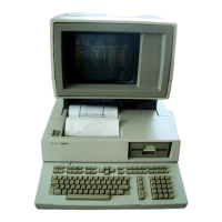
to the
computer mainframe_ The connectors are as follows:
Jl
- 36-pin; alpha data to the display
J2
- 50-pin; power to the
DIM
J3
- 36-pin; graphics data to the display
J4
- 50-pin; lOP bus to the
DIM
Interface Buffers
The interface buffers between the lOP bus
and
the combined alpha/graphics minimize capacitive
loading
on
the lOP signal lines. Data
and
control signals from the buffers split into
an
alpha path
and
a graphics path.
Graphics data
and
control information are transferred directly to the display. Alpha data
is
gated
into the alpha data buffer.
Control signals are also exchanged between the interface buffers
and
the controller. The output-
status-flag-enable
(OSFE) signal enables Status
and
Flag to the lOP bus.
The lower 8 lines of the data bus provide an 8-bit-wide data path between the interface buffers
and
the controller. This path
is
used to transfer address, control,
and
data information.
Alpha Data Buffer
The alpha data buffer provides isolation between the interface buffers
and
the frame buffer when
the display
is
being refreshed
or
the line buffer
is
being loaded.
With
DIR,
the controller determines the direction of data through the buffer. Data
is
normally
written to the buffer from the
lOP. However, the lOP bus can read data from frame buffer memory
via the alpha data
and
interface buffers to test data integrity.