2-38
Theory
of
Operation
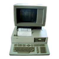
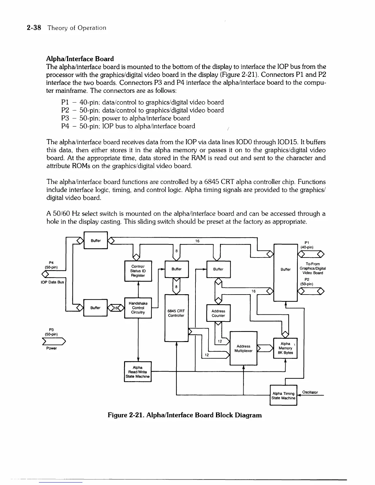
Alpha/Interface Board
The alpha/interface board
is
mounted to the bottom of the display to interface the lOP bus from the
processor with the graphics/digital video board
in
the display (Figure 2-21). Connectors P1
and
P2
interface the two boards. Connectors P3
and
P4
interface the alpha/interface board to the compu-
ter mainframe. The connectors are as follows:
P1
- 40-pin; data/control to graphics/digital video board
P2 - 50-pin; data/control to graphics/digital video board
P3 - 50-pin; power to alpha/interface board
P4
- 50-pin; lOP bus to alpha/interface board
The alpha/interface board receives data from the
lOP via data lines
1000
through
10015.
It
buffers
this data, then either stores
it
in
the alpha memory or passes
it
on to the graphics/digital video
board.
At
the appropriate time, data stored
in
the
RAM
is
read out
and
sent to the character
and
attribute ROMs
on
the graphics/digital video board.
The alpha/interface board functions are controlled by a 6845 CRT alpha controller chip. Functions
include interface logic, timing, and control
logic.
Alpha timing signals are provided to the graphics/
digital video board.
A
50/60
Hz
select switch
is
mounted on the alpha/interface board and can be accessed through a
hole
in
the display casting. This sliding switch should
be
preset at the factory as appropriate.
P4
(50-pin)
lOP Data Bus
P3
(50-pin)
) )
Power
P1
(40-pin)
To/From
Buffer Graphics/Digital
Handshake
Control
Circuitry
Alpha
ReadlWrite
State Machine
12
16
,------,
Alpha \
Memory
8K
Bytes
'"----------...L.------f
Alpha Timing
State Machine
Figure 2-21. Alpha/Interface Board Block Diagram
Video Board
P2
(50-pin)
Oscillator