2-18
Theory
of
Operation
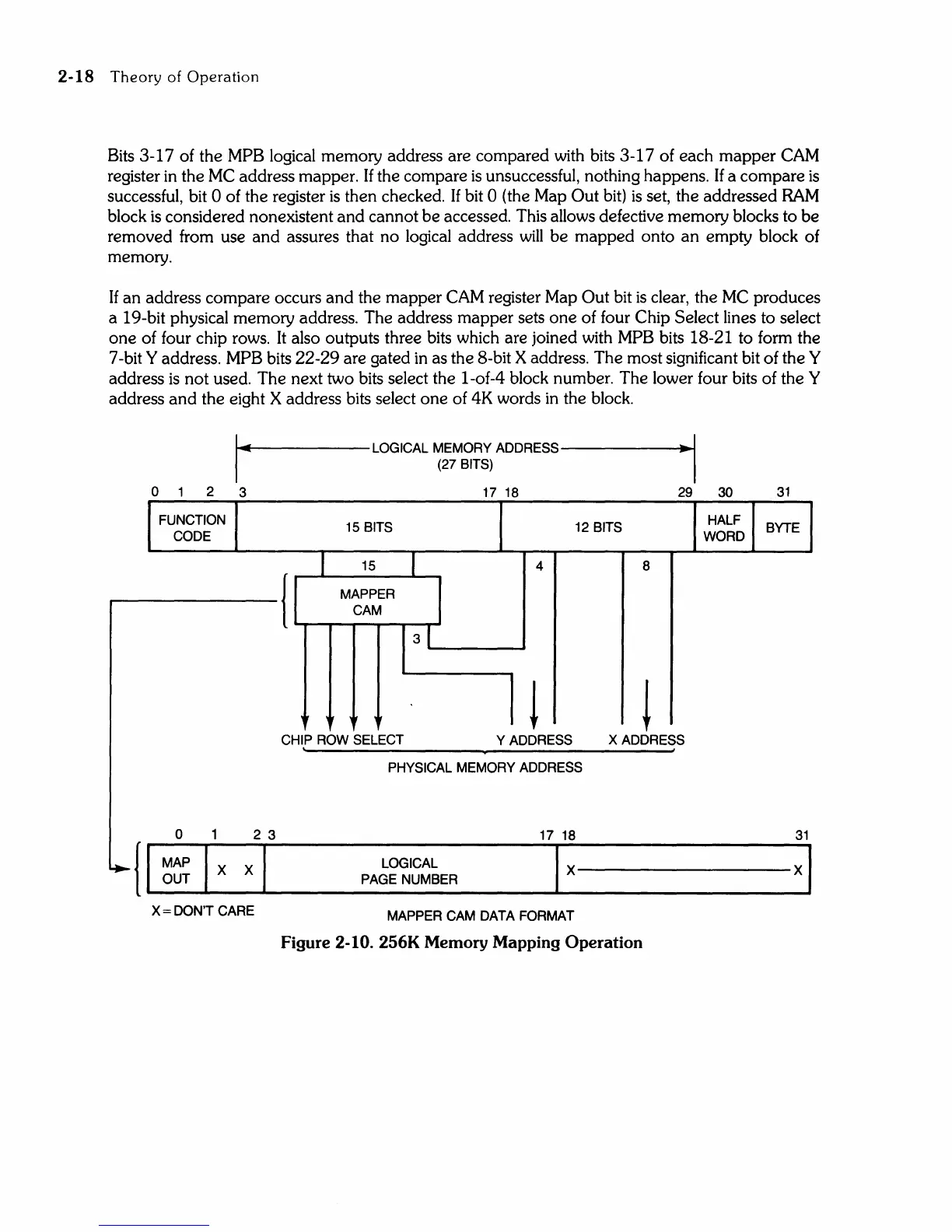
Bits 3-1 7 of the MPB logical memory address are compared with bits 3-1 7 of each
mapper
CAM
register
in
the
MC
address mapper. If the compare
is
unsuccessful, nothing happens.
If
a compare
is
successful, bit 0 of the register
is
then checked.
If
bit 0 (the Map Out
bit)
is
set, the addressed
RAM
block
is
considered nonexistent
and
cannot
be
accessed. This allows defective memory blocks to
be
removed from use
and
assures that no logical address
will
be
mapped onto
an
empty block of
memory.
If
an address compare occurs
and
the mapper
CAM
register Map Out bit
is
clear, the
MC
produces
a 19-bit physical memory address. The address mapper sets
one
of four Chip Select lines to select
one
of four chip rows. It also outputs three bits which are joined with MPB bits 18-21 to form the
7 -bit
Y address. MPB bits 22-29 are gated
in
as the 8-bit X address. The most significant bit of the Y
address
is
not used. The next two bits select the 1-of-4 block number. The lower four bits of the Y
address
and
the eight X address bits select
one
of 4K words
in
the block.
o
i
....
.-------LOGICAL
MEMORY
ADDRESS-----~
.... I
(27
BITS)
2 3
17
18
29
30
FUNCTION
15
BITS
12
BITS
HALF
CODE
WORD
I
15
I
4
8
{
MAPPER
CAM
3 I
,
,.
,
. ,
!
!
CHIP
ROW
SELECT
Y
ADDRESS
X
ADDRESS
.
,
PHYSICAL
MEMORY
ADDRESS
31
BYTE
o 1 2 3
17
18
31
LOGICAL
PAGE
NUMBER
x = DON'T
CARE
MAPPER
CAM
DATA
FORMAT
Figure 2-10. 256K Memory Mapping Operation