Theory
of
Operation
2-23
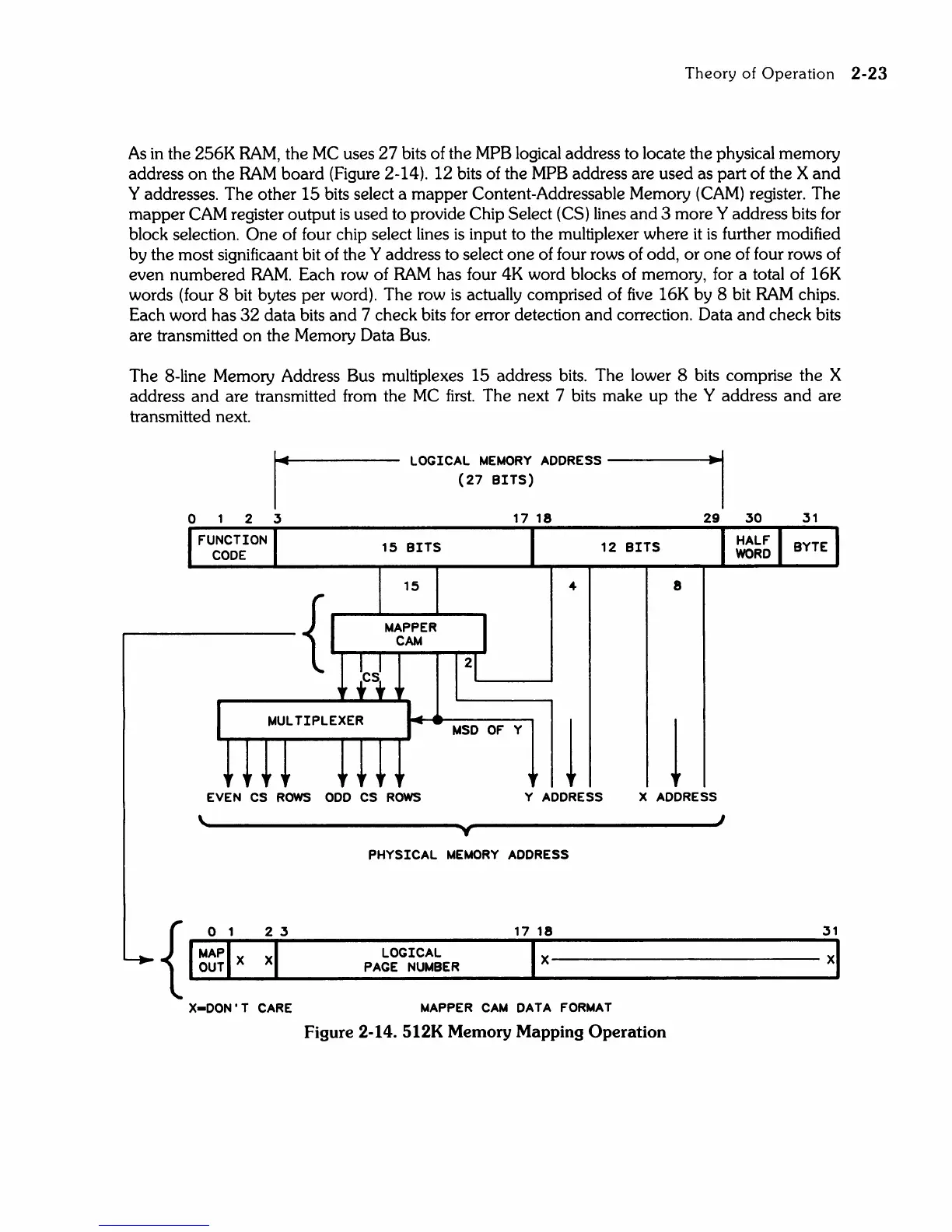
As
in the 256K
RAM,
the
MC
uses
27
bits of the MPB logical address to locate the physical memory
address
on
the
RAM
board (Figure 2-14). 12 bits of the MPB address are used as part of the X
and
Yaddresses. The other
15
bits select a mapper Content-Addressable Memory
(CAM)
register.
The
mapper
CAM
register output
is
used to provide Chip Select (CS) lines
and
3 more Y address bits for
block selection.
One
of four chip select lines
is
input to the multiplexer where
it
is
further modified
by the most significaant bit of the
Y address to select
one
of four rows of odd, or
one
of four rows of
even numbered
RAM.
Each row of
RAM
has four 4K word blocks of memory, for a total of 16K
words (four 8 bit bytes per word). The row
is
actually comprised of
five
16K by 8 bit
RAM
chips.
Each word has
32
data bits
and
7 check bits for error detection
and
correction. Data
and
check bits
are transmitted
on
the Memory Data Bus.
The 8-line Memory Address Bus multiplexes 15 address bits. The lower 8 bits comprise the X
address
and
are transmitted from the
MC
first.
The next 7 bits make up the Y address
and
are
transmitted next.
I~
LOGICAL
MEMORY
ADDRESS~
(27
BITS)
I
o
2 3
17
18
29
30
31
15 BITS 12 BITS
15
8
~--------------_1[~~~M~~_~_E_R~~2~
\
MSD
OF
Y
!
!
EVEN
CS
ROWS
ODD
CS
ROWS
Y
ADDRESS
X
ADDRESS
y
I
PHYSICAL
MEMORY
ADDRESS
17
18
31
LOGICAL
PAGE
NUMBER
Ix-----xl
MAPPER
CAM
DATA
FORMAT
Figure 2-14. 512K Memory Mapping Operation