67
Output Unit Specifications Section 2-3
Details of Changes Output elements have been changed from NPN transistors to field-effect tran-
sistors (FET). Part of the circuit configuration has been changed. There are
no changes in performance characteristics as a result of these improvements.
Manufacturing Numbers
Terminal Connections
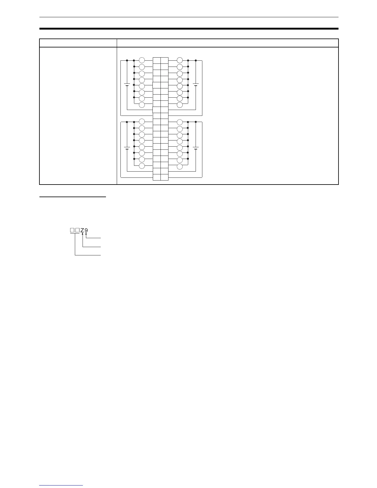
Item CQM1-OD213
The COM terminals are internally con-
nected, but they all must be wired.
4 4
5 5
6 6
7 7
8 8
9 9
11 11
12 12
13 13
14 14
15 15
16 16
17 17
18 18
3 3
2 2
19 19
20 20
1 1
COM
COM
OUT0
OUT1
OUT2
OUT3
OUT4
OUT5
OUT6
OUT7
10 10
COM
OUT8
OUT9
OUT10
OUT11
OUT12
OUT13
OUT14
A B
++
+
+
Wd m Wd (m+1)
L
L
L
L
L
L
L
L
L
L
L
L
L
L
L
L
L
L
L
L
L
L
L
L
L
L
L
L
L
L
L
L
L
L
L
L
L
L
OUT15
L
COM
L
4.5 to
26.4 V DC
+DC +DC
+DC +DC
OUT0
OUT1
OUT2
OUT3
OUT4
OUT5
OUT6
OUT7
OUT8
OUT9
OUT10
OUT11
OUT12
OUT13
OUT14
OUT15
Note Do not reverse the polarity of
the load power supply. If the
load power supply is con-
nected incorrectly, the loads
may not operate correctly.
((
Z9
Year: Last digit of calendar year; e.g., 1999→9, 2000→0
Month: 1 to 9 (January to September), X (October), Y (November), Z (December)
Day: 01 to 31
 Loading...