13 Hardware Examples
13 – 6
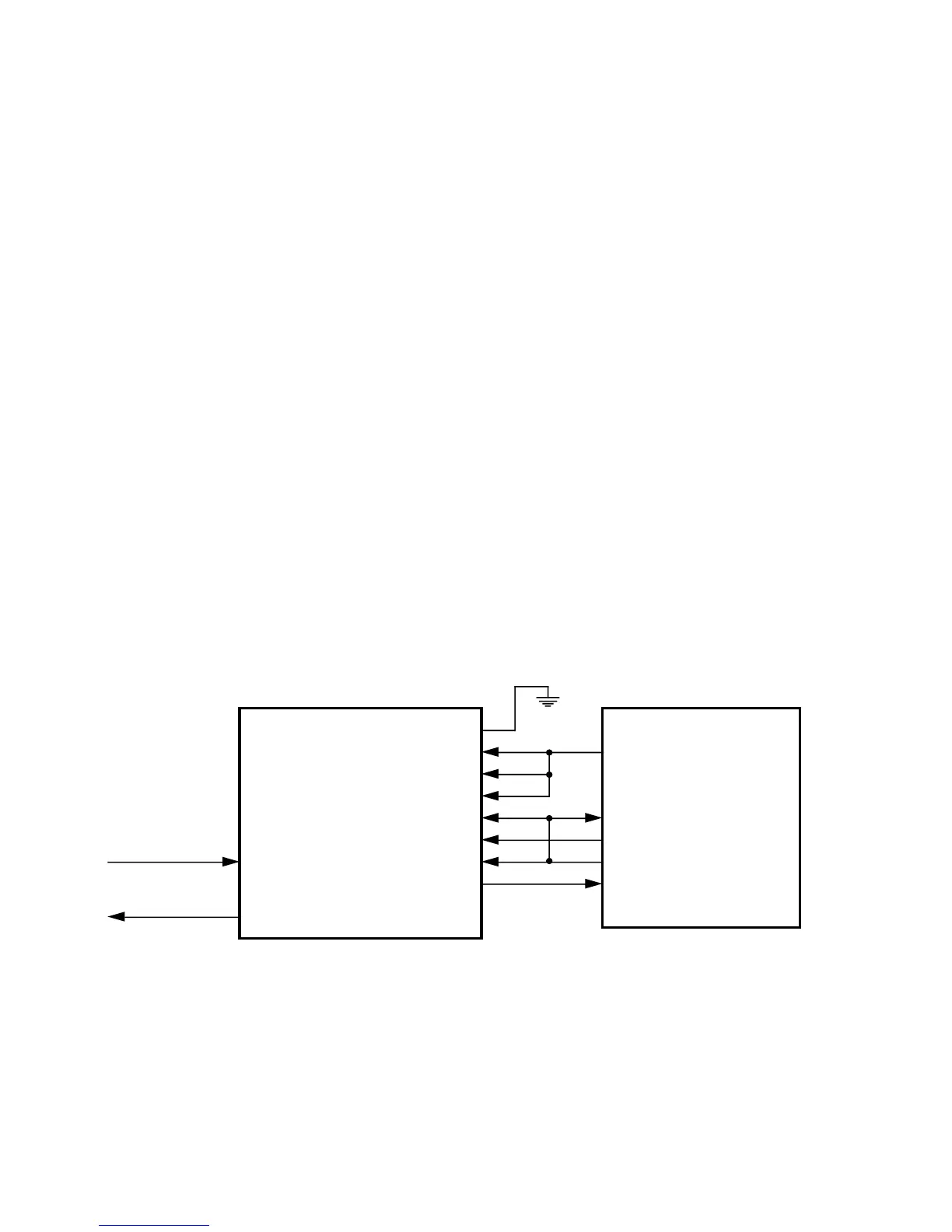
Figure 13.2 shows an industry standard µ-law companding codec
connected to a serial port (in this case, SPORT0) on an ADSP-21xx
processor. The codec’s analog input at VFXI+ is internally amplified by a
gain which is controlled by the resistor combination at GSX and VFXI–.
The gain is
20 x log (R1 + R2)/R2
in this case, 20 log 2.
The ADSP-21xx controls codec operation by supplying master and bit
clock signals. In the configuration shown, the codec transmit and receive
sections operate synchronously. MCLKR and MCLKX are the master
clocks for the receive and transmit sections of the codec, respectively.
BCLKX is the bit clock and in this configuration is used for clocking both
received and transmitted serial data. MCLKR, MCLKX and BCLKX must
be synchronous and in this case they are the same signal, namely the
SCLK0 output generated by the ADSP-21xx processor. The BCLKR/
CLKSEL input, tied low, selects the frequency of MCLKX to be 2.048 MHz.
The ADSP-21xx must be programmed for internal SCLK0 generation at
2.048 MHz.
CODEC
(National
Seminconductor
TP3054)
BCLKR/CLKSEL
MCLKR
BCLKX
MCLKX
FSR
DR
FSX
DX
VFRO
VFXI+
TFS0
DT0
RFS0
DR0
SCLK0
ADSP-21xx
(Serial Port 0)
From Input
Amplifier
To Output
Amplifier
Digital
Ground
Figure 13.2 ADSP-21xx Serial Port (SPORT0) To CODEC

 Loading...

