EControl/Status Registers
E – 1
E.1 OVERVIEW
This appendix shows bit definitions for 1) the memory-mapped control
registers and 2) other (non-memory-mapped) control and status registers
of all ADSP-21xx processors. The memory-mapped registers are listed in
descending address order. Default bit values at reset are shown; if no
value is shown, the bit is undefined at reset. Reserved bits are shown on a
gray field. These bits should always be written with zeros.
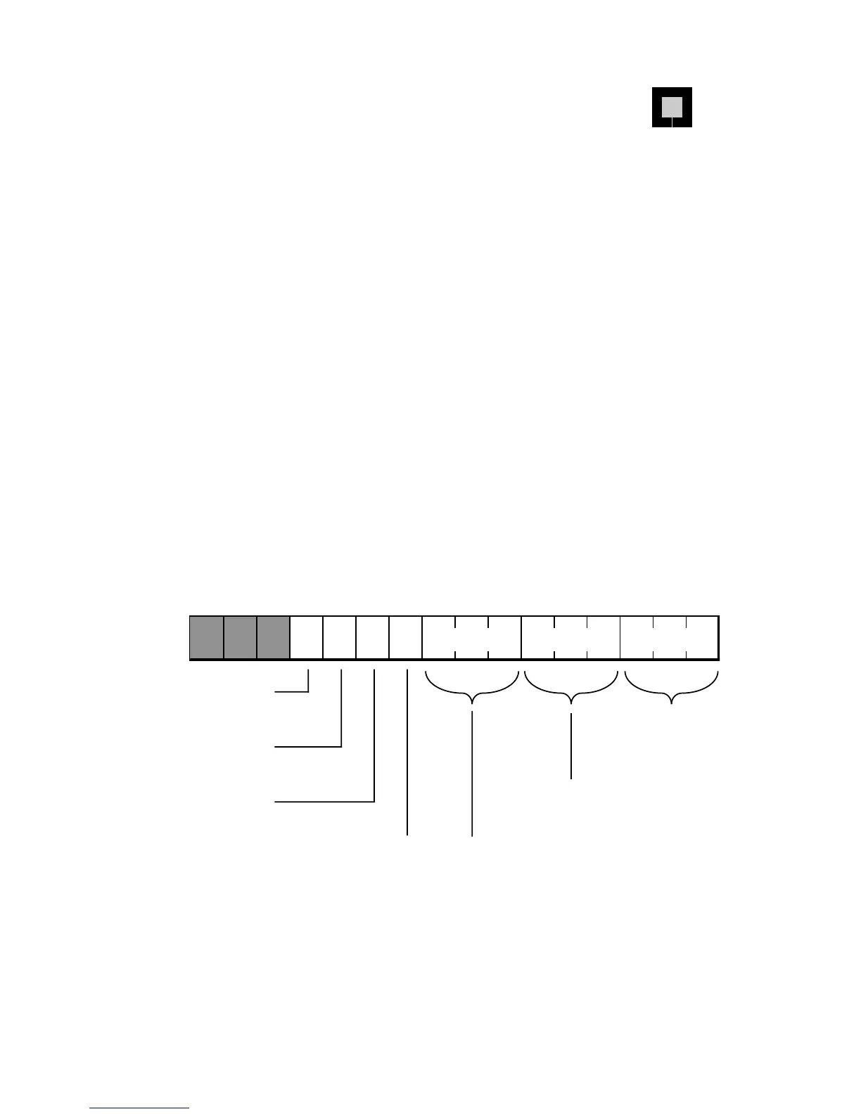
15 14 13 12 11 10 9 8 7 6 5 4 3 2 1 0
BPAGE
Boot Page Select
(not on ADSP-2181)
BWAIT
Boot Wait States*
(not on ADSP-2181)
BFORCE
Boot Force Bit
(not on ADSP-2181)
PWAIT
Program Memory
Wait States
0100
SPORT0 Enable
1 = enabled, 0 = disabled
(set to 0 for ADSP-2105)
SPORT1 Enable
1 = enabled, 0 = disabled
SPORT1 Configure
1 = serial port
0 = FI, FO, IRQ0, IRQ1, SCLK
000
111*11000
* Bit 5 initialized to 1 on ADSP-2171, ADSP-21msp58/59
Bit 5 initialized to 0 on ADSP-2101, ADSP-2105, ADSP-2115, ADSP-2111
System Control Register
Memory-Mapped Registers
DM(0x3FFF)

 Loading...

