11 DMA Ports
11 – 18
Note: The IDMA starting address and destination memory type is available to
the host and to the ADSP-2181 in the IDMA Control Register. For Data Memory
accesses, the ADSP-2181 increments the address automatically after each IDMA
read or write transfer (16-bit word). For Program Memory accesses, the
ADSP-2181 increments the address automatically after each pair of IDMA read
or write transfers (24-bit word).
Warning: Both the ADSP-2181 and the host can specify the starting address by
writing to the IDMA Control Register. Do not let the ADSP-2181 access the
IDMA Control Register while it is being written by the host; this operation will
have an indeterminate result.
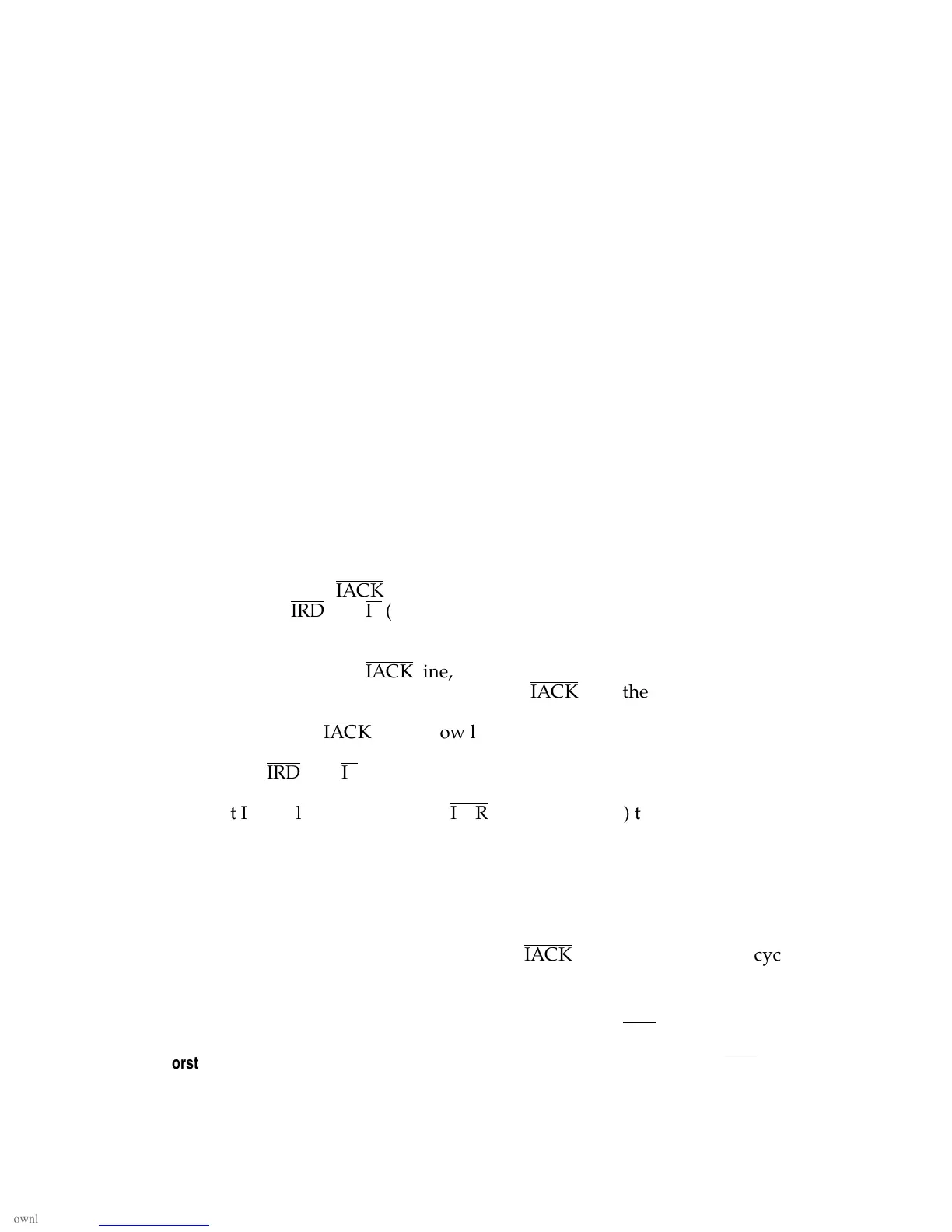
11.3.4.2 Long Read Cycle
The host reads the contents of an ADSP-2181 internal memory location using
the IDMA port long read cycle. The read cycle, shown in Figure 11.10, consists
of the following steps:
1. Host ensures that
IACK
line is low.
2. Host asserts
IRD
and
IS
(low), causing the ADSP-2181 to put the contents of
the location pointed to by the IDMA address on the IAD15-0 address/data
bus.
3. ADSP-2181 deasserts
IACK
line, indicating the requested data is being
fetched. When the ADSP-2181 asserts the
IACK
line, the requested data is
driven on the IAD address/data bus.
4. Host detects the
IACK
line is now low and reads the data (READ DATA)
from the IAD15-0 address/data bus. After reading the data, the host
deasserts
IRD
and
IS
.
Note that IAL is low (inactive) and
IWR
is high (inactive) throughout the read
operation.
IDMA memory accesses “steal” one processor cycle, but may only occur on
instruction cycle boundaries. The best-case response for a 16-bit Data Memory
read or the first 16 bits of a Program Memory read is 2.5 processor cycles; worst
case is 3.5 cycles. One cycle is for synchronization, one is for reading the
memory internally, and one-half cycle is for
IACK
setup time. A second cycle of
synchronization may be required. Thus the best-case and worst-case response
times are determined as follows:
Best Case: 1 cycle (sync) + 1 cycle (internal memory read) + 0.5 cycle (
IACK
setup) = 2.5 cycles
Worst Case: 1 cycle (sync) + 1 cycle (sync) + 1 cycle (internal memory read) + 0.5 cycle (
IACK
setup) = 3.5 cycles

 Loading...

