8 Analog Interface
8 – 10
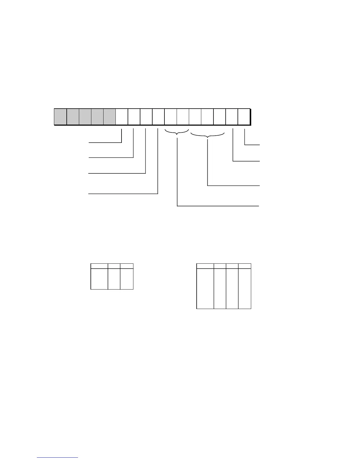
1514131211109876543210
DM[0x3FEE]
DABY
DAC High Pass Filter Bypass
1=bypass, 0=insert
APWD
Analog Interface Powerdown
0=powerdown, 1=enable
(Set both bits to 1 to
enable analog interface)
0000000
ADBY
ADC High Pass Filter Bypass
1=bypass, 0=insert
Analog Control Register
IG1
ADC Input Gain (ADC PGA)
IMS
ADC Input Multiplexer Select
1=AUX input, 0=NORM input
OG0OG1OG2
OG2, OG1, OG0
DAC Output Gain (DAC PGA)
Gain
+6 dB
+3 dB
0 dB
–3 dB
–6 dB
–9 dB
–12 dB
–15 dB
OG2
0
0
0
0
1
1
1
1
OG1
0
0
1
1
0
0
1
1
OG0
0
1
0
1
0
1
0
1
All bits are set to 0 at processor reset.
(Reserved bits 10-15 must always be set to 0.)
000000000
IG0
ADC Input Gain (ADC PGA)
OG2, OG1, OG0
DAC Output Gain (DAC PGA)
Gain
0 dB
+6 dB
+20 dB
+26 dB
IG1
0
0
1
1
IG0
0
1
0
1
IG1, IG0
ADC Input Gain (ADC PGA)
ADC Offset
DM(0x3FEE)
Figure 8.4 Analog Control Register
8.4.1.2 Analog Autobuffer/Powerdown Register
The analog autobuffer/powerdown register (located at address 0x3FEF
in data memory) is shown in Figure 8.5. This register enables or
disables autobuffering of ADC receive data and/or DAC transmit
data—autobuffering is enabled by writing ones to the ARBUF (bit 0)
and/or ATBUF (bit 1) bits. When autobuffering is enabled, I (index)
and M (modify) registers are selected in bits 2–11 for the receive
and/or transmit data buffers. See “Autobuffering” in the Serial Ports
chapter for details on autobuffering.

 Loading...

