10 Memory Interface
10 – 14
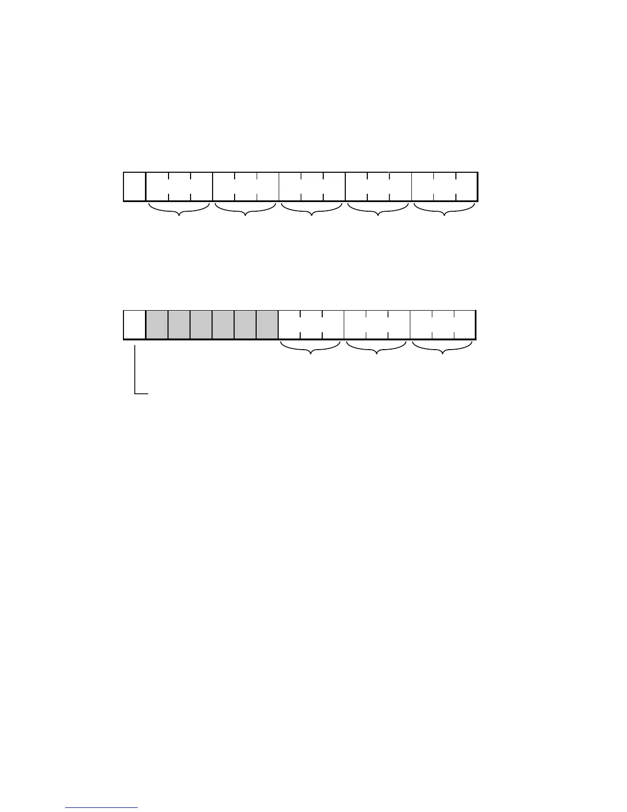
1514131211109876543210
DWAIT0DWAIT1DWAIT2DWAIT3DWAIT4
0
111111111111111
DM(0x3FFE)
Figure 10.15 Data Memory Waitstate Control Register (ADSP-2171/72, ADSP-21msp58/59)
Figure 10.14 Data Memory Waitstate Control Register (ADSP-2101, ADSP-2111,
ADSP-2105, ADSP-2115, ADSP-2161/62/63/64)
ROM Enable (ADSP-2172, ADSP-21msp59 only)
1=enable
0=disable
1514131211109876543210
DWAIT0DWAIT1DWAIT2
0111111111000000
DM(0x3FFE)
10.3.3 Memory-Mapped Peripherals
Peripherals requiring parallel communications and other types of devices
can be mapped into external data memory. Communication takes the form
of reading and writing the memory locations associated with the device.
Some A/D and D/A converters require this type of interface. The .PORT
directives in the System Builder and Assembler modules of the ADSP-2100
Family Development Software support this mapping.
Communication with a memory-mapped device consists simply of reading
and writing the appropriate locations. By matching the access times of the
external devices to the wait states specified for their zone of data memory,
you can easily interface a variety of devices.
The 16 MSBs of the external data bus (D
23-8
) are connected to the 16 LSBs of
the internal DMD bus, so D
23-8
should be used for 16-bit peripherals.

 Loading...

