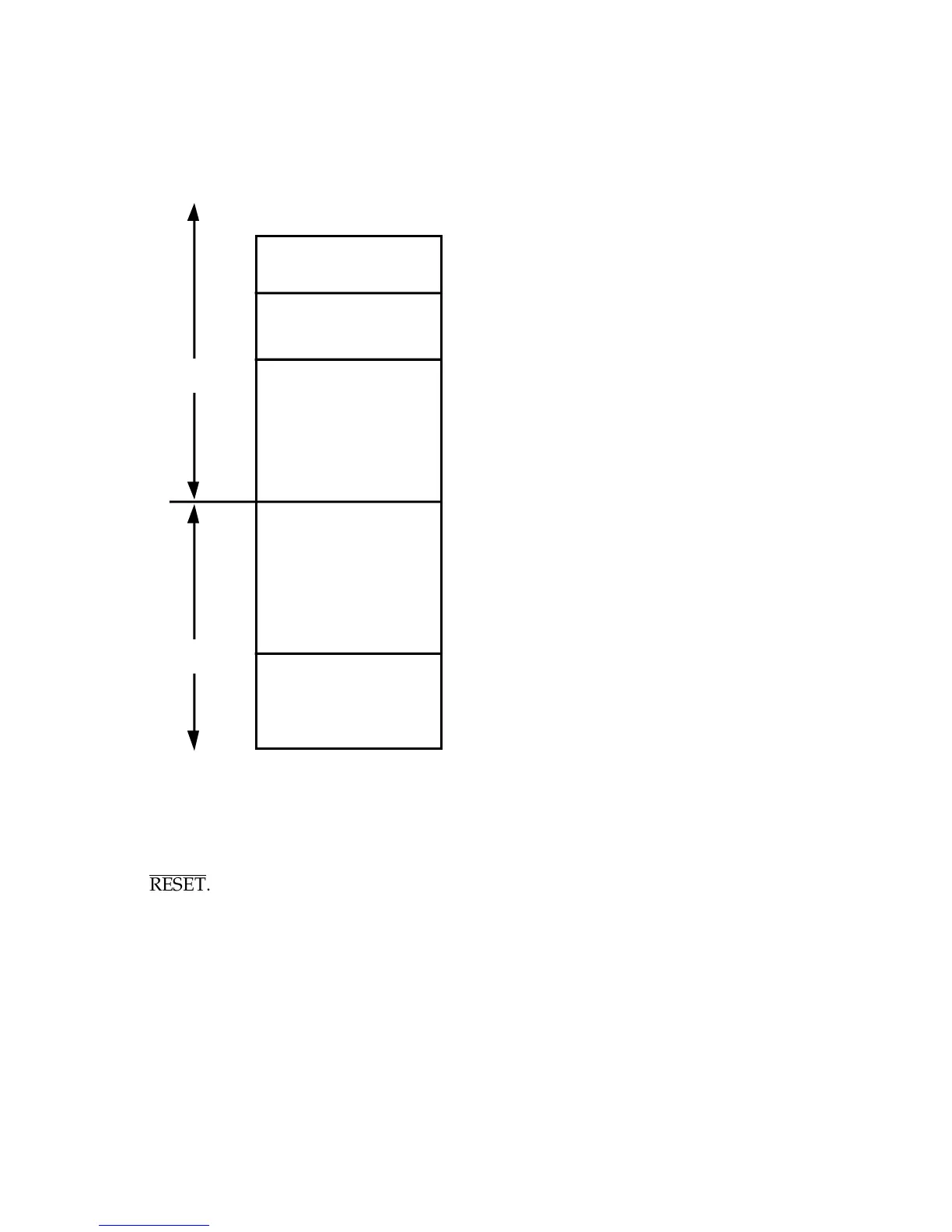
10Memory Interface
10 – 13
Memory Mapped
Registers
and Reserved
0x3000
0x0400
0x3FFF
0x0000
1K External
DWAIT0
1K External
DWAIT1
6K External
DWAIT2
0x2000
0x0800
4K x 16 Internal
EXTERNAL
RAM
INTERNAL
RAM
4K x 16
Figure 10.13 Data Memory Map (ADSP-2165/66)
The Data Memory Waitstate control register has a separate field for each zone
of external memory. Each 3-bit field specifies the number (0-7) of wait states
for the corresponding zone of memory; all zones default to 7 wait states after
RESET
. Figure 10.14 shows this control register for the ADSP-2101, ADSP-2111,
ADSP-2105, ADSP-2115, and ADSP-2161/62/63/64 processors. Figure 10.15
shows the register for the ADSP-2171/72 and ADSP-21msp58/59 processors;
on the ADSP-2172 and ADSP-21msp59, one bit in this register is used to enable
or disable the on-chip ROM.

 Loading...

