10 Memory Interface
10 – 36
CMS
signal. In this system the
CMS
line drives the chip select for all
three SRAMs. This lets you use three 32K x 8-bit SRAMs, with no glue
logic, for complete program and data memory overlays.
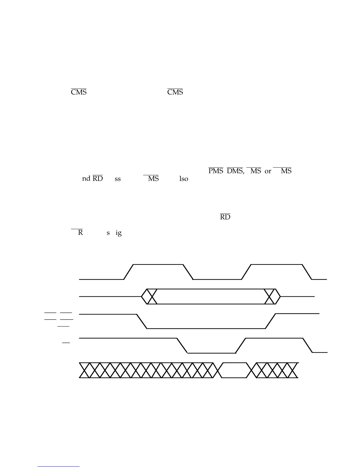
10.6.6 External Memory Read – Overlays & I/O Memory
External memory reads may access either PM overlays, DM overlays, or
I/O memory space. These read operations occur in the following
sequence (see Figure 10.34):
1) The ADSP-2181 executes a read from an external memory address; the
address is driven on the address bus and
PMS
,
DMS
,
BMS
, or
IOMS
,
and
RD
is asserted. (
CMS
may also be asserted, depending how it is
configured.)
2) The external peripheral drives the data onto the data bus.
3) The ADSP-2181 reads the data and deasserts
RD
.
WR
remains high (deasserted) throughout the external memory read
operation.
Note that ADSP-2181 internal memory accesses do not drive any
CLKOUT
A0 – A13
DATA
RD
DMS, PMS,
BMS, IOMS,
or
CMS
Figure 10.34 External Memory Read Timing

 Loading...

