7 Host Interface Port
7 – 12
7.6 HOST
INTERFACE TIMING
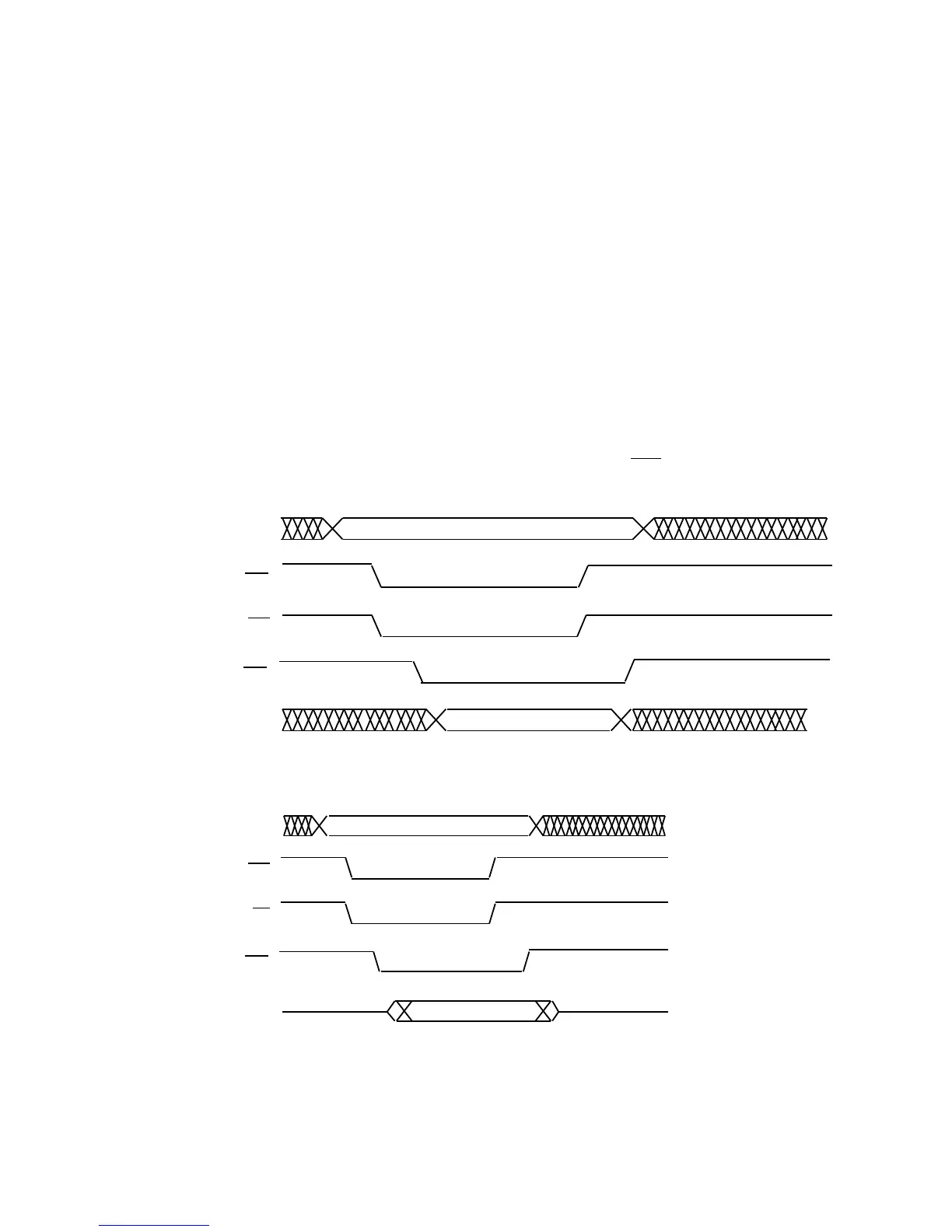
The following diagrams show the timings of HIP signals in the various
modes determined by HMD0 and HMD1. HMD0 configures the bus
strobes, selecting either separate read and write strobes or a single read/
write select and a host data strobe. HMD1 configures the bus protocol,
selecting either separate address (3-bit) and data (16-bit) buses or a
multiplexed 16-bit address/data bus with address latch enable. The
HSIZE pin can be changed on a cycle-by-cycle basis; although not shown
in the following diagrams, it has the same timing as the H
RD/HRW signal.
Figure 7.6 shows the HIP timing when both HMD0=0 and HMD1=0.
HD15–0
HSEL
HWR
HACK
HA2–0
DATA
ADDRESS
HSEL
HRD
HACK
HA2–0 ADDRESS
HD15–0
DATA
Host Write Cycle
Host Read Cycle
Figure 7.6 HIP Timing: Separate Strobes, Separate Buses

 Loading...

