10 Memory Interface
10 – 32
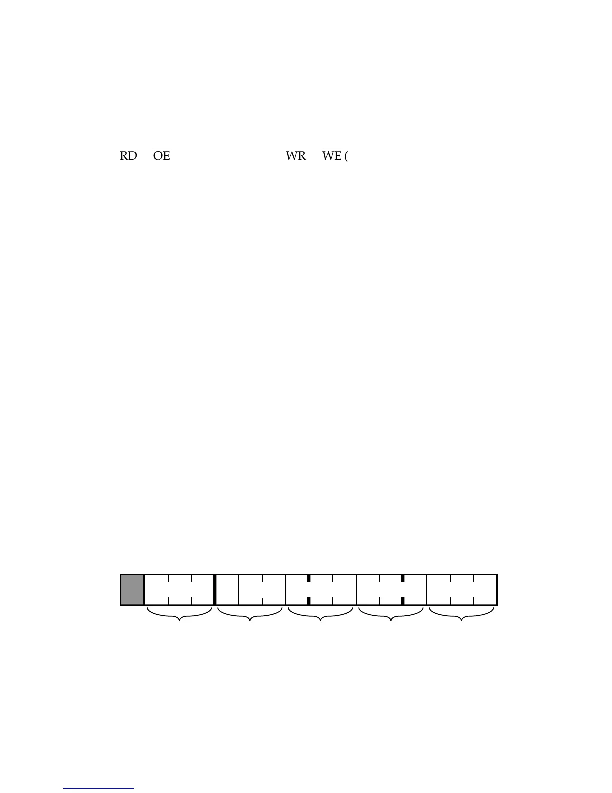
RD
to
OE
(Output Enable) and
WR
to
WE
(Write Enable) of your memory.
10.6.3 ADSP-2181 Byte Memory Interface
The ADSP-2181’s byte memory space is 8 bits wide and can address up to
4M bytes of program code or data. This memory space takes the place of
the boot memory space found on other ADSP-2100 family processors.
Unlike boot memory space, byte memory has read/write access through
the ADSP-2181’s BDMA port.
Byte memory space consists of 256 pages, each containing 16K x 8-bit wide
locations. This memory can be written and read in four different formats:
24-bit, 16-bit, 8-bit MSB alignment, and 8-bit LSB alignment.
Each read/write to byte memory consists of data (on data bus lines 15:8)
and address (on address bus lines 13:0 plus data lines 23:16). The 22-bit
byte memory address lets you access up to 4M bytes of ROM or RAM.
For complete information on the ADSP-2181’s byte memory and BDMA
port, refer to the DMA Ports chapter of this manual.
10.6.4 ADSP-2181 I/O Memory Space
The ADSP-2181 has a dedicated I/O Memory Space instead of the
memory-mapped I/O used on other ADSP-21xx processors. The I/O
memory space consists of 2048 locations with four associated
programmable waitstate regions. Figure 10.30 shows the Wait State
1514131211109876543210
IOWAIT0IOWAIT1IOWAIT2IOWAIT3DWAIT
0 111111111111111
DM(0x3FFE)
Wait State Control Register
Figure 10.30 ADSP-2181 Waitstate Control Register

 Loading...

