EasyManua.ls Logo

Analog Devices adsp-2100 User Manual

Analog Devices adsp-2100
486 pages
To Next Page IconTo Next Page
To Previous Page IconTo Previous Page
Page #426 background imageLoading...
Page #426 background image
15
15 – 103
Syntax:
AX0 = DM ( I0 , M0 ) , AY0 = PM ( I4 , M4 ) ;
AX1 I1 M1 AY1 I5 M5
MX0 I2 M2 MY0 I6 M6
MX1 I3 M3 MY1 I7 M7
Description: Perform the designated memory reads, one from data
memory and one from program memory. Each read operation moves the
contents of the memory location to the destination register. For this double
data fetch, the destinations for data memory reads are the X registers in
the ALU and the MAC, and the destinations for program memory reads
are the Y registers. The addressing mode for this memory read is register
indirect with post-modify. For linear (i.e. non-circular) indirect
addressing, the L register corresponding to the I register used must be
set to zero. The contents of the source are always right-justified in the
destination register.
A multifunction instruction requires three items to be fetched from
memory: the instruction itself and two data words. No extra cycle is
needed to execute the instruction as long as only one of the fetches is from
external memory.
If two off-chip accesses are required, however—the instruction fetch and
one data fetch, for example, or data fetches from both program and data
memory—then one overhead cycle occurs. In this case the program
memory access occurs first, then the data memory access. If three off-chip
accesses are required—the instruction fetch as well as data fetches from
both program and data memory—then two overhead cycles occur.
Status Generated: No status bits are affected.
Instruction Format:
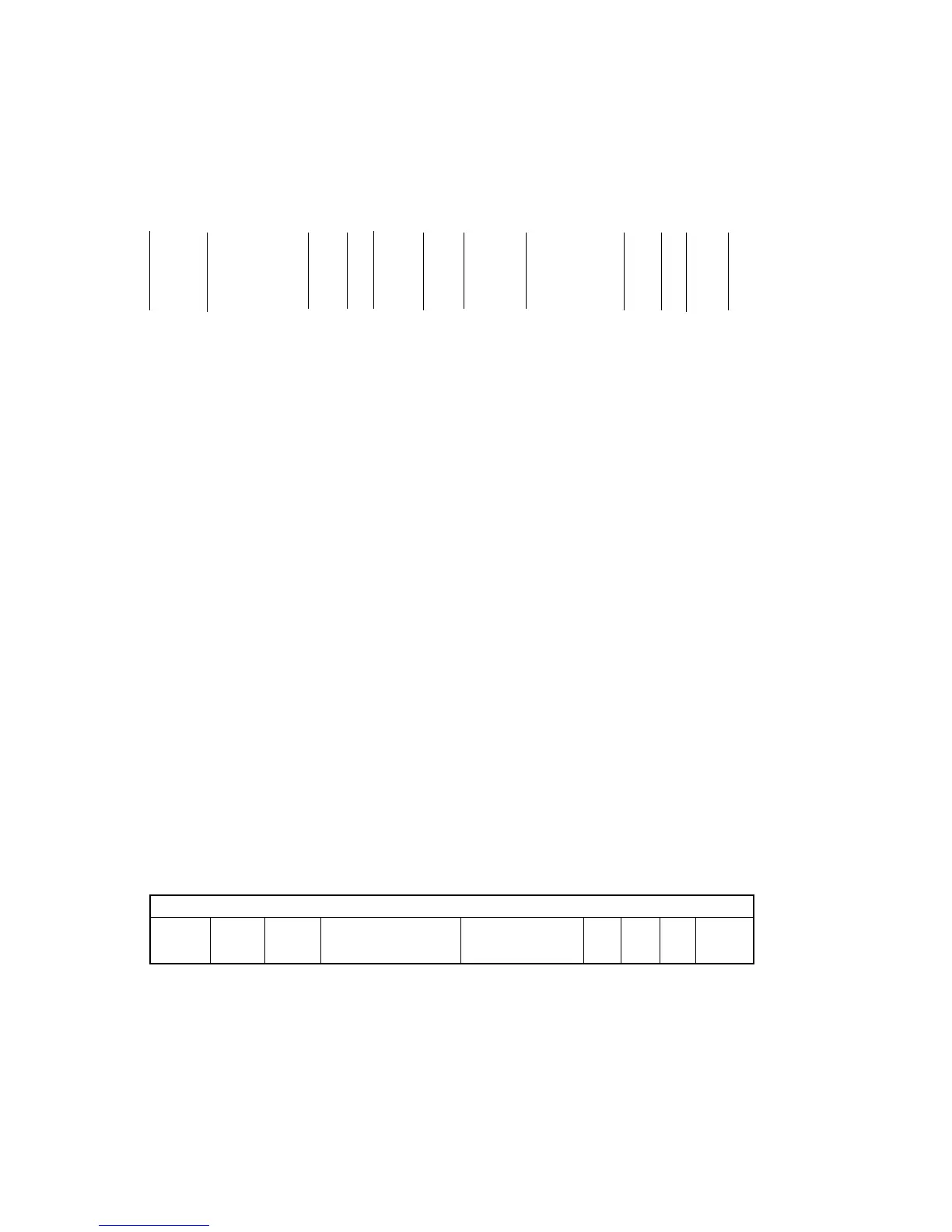
ALU/MAC with Data & Program Memory Read, Instruction Type 1:
23 22 21 20 19 18 17 16 15 14 13 12 11 10 9 8 7 6 5 4 3 2 1 0
1 1 PD DD AMF 0 0 0 0 0 PM PM DM DM
I M I M
AMF specifies the ALU or MAC function. In this case, AMF = 00000,
designating a no-operation for the ALU or MAC function.
PD: Program Destination register DD: Data Destination register
AMF: ALU/MAC operation I: Indirect address register
M: Modify register
MULTIFUNCTION
DATA & PROGRAM MEMORY READ

Table of Contents

Question and Answer IconNeed help?

Do you have a question about the Analog Devices adsp-2100 and is the answer not in the manual?

Analog Devices adsp-2100 Specifications

General IconGeneral
CategoryDigital Signal Processor (DSP)
Word Length16 bits
Instruction Word Width24 bits
Data Bus Width16 bits
Address Bus Width24 bits
Accumulator Size40 bits
Operating Voltage5 V
Manufacturing ProcessCMOS
ArchitectureHarvard Architecture
Clock Speed10 MHz
On-Chip RAM512 words
PackagePQFP
Multiplier Size16x16-bit
I/O Ports8-bit parallel I/O port

Summary

CHAPTER 1 INTRODUCTION

1.1 OVERVIEW

Introduction to the ADSP-2100 family architecture, DSP optimization, and manual scope.

1.2 CORE ARCHITECTURE

Describes the core components: ALU, MAC, Shifter, DAGs, Program Sequencer.

CHAPTER 2 COMPUTATIONAL UNITS

2.1 OVERVIEW

Introduces the three computational units: ALU, MAC, and Barrel Shifter, and number formats.

2.2 ARITHMETIC/LOGIC UNIT (ALU)

Details the ALU's standard arithmetic and logic functions.

2.3 MULTIPLIER/ACCUMULATOR (MAC)

Covers MAC's high-speed multiplication, accumulation, and saturation functions.

2.4 BARREL SHIFTER

Describes the shifter's functions: arithmetic, logical shifts, normalization, exponent derivation.

CHAPTER 3 PROGRAM CONTROL

3.1 OVERVIEW

Describes the program sequencer, interrupt controller, and status/condition logic.

3.2 PROGRAM SEQUENCER

Explains how the sequencer generates instruction addresses and controls program flow.

3.4 INTERRUPTS

Explains how the program sequencer responds to interrupts by vectoring to appropriate addresses.

3.4.2 Configuring Interrupts

Details registers used for interrupt configuration: ICNTL, IMASK, IFC.

3.5 STATUS REGISTERS & STATUS STACK

Describes status registers (ASTAT, SSTAT, MSTAT) and the status stack.

CHAPTER 4 DATA TRANSFER

4.1 OVERVIEW

Describes processor units controlling data movement and bus exchange.

4.2 DATA ADDRESS GENERATORS (DAGS)

Explains the two independent DAGs for indirect addressing and automatic address modification.

CHAPTER 5 SERIAL PORTS

5.1 OVERVIEW

Describes synchronous serial ports (SPORTS) for serial data communications and interconnections.

5.3 SPORT PROGRAMMING

Describes programming SPORT configuration registers and data section.

5.3.1 SPORT Configuration

Explains how to accomplish SPORT configuration by setting bit and field values in registers.

5.11 AUTOBUFFERING

Details autobuffering mechanism for receiving/transmitting entire data blocks.

CHAPTER 6 TIMER

6.1 OVERVIEW

Introduces the programmable interval timer for generating periodic interrupts.

6.2 TIMER ARCHITECTURE

Details timer registers TCOUNT, TPERIOD, TSCALE, and mode control.

CHAPTER 7 HOST INTERFACE PORT

7.1 OVERVIEW

Introduces HIP as a parallel I/O port for using processors as memory-mapped peripherals.

7.3 HIP FUNCTIONAL DESCRIPTION

Details HIP's three functional blocks: HCI, data registers (HDRs), and status registers (HSRs).

7.4 HIP OPERATION

Explains how the ADSP-21xx core and host computer interact via HDRs.

7.5 HIP INTERRUPTS

Covers HIP interrupts, their masking via IMASK/HMASK, and vector locations.

7.7 BOOT LOADING THROUGH THE HIP

Explains loading internal program RAM using a boot sequence via HIP.

CHAPTER 8 ANALOG INTERFACE

8.1 OVERVIEW

Introduces the analog signal interface with ADC, DAC, filters, and registers.

8.2 A/D CONVERSION

Details the A/D conversion circuitry including input multiplexer, PGA, and ADC.

8.2.2 ADC

Describes the ADC components: sigma-delta modulator, decimation filter, and digital high pass filter.

8.3 D/A CONVERSION

Covers the D/A conversion circuitry including DAC, smoothing filter, PGA, and output amplifier.

8.3.1 DAC

Details the DAC's digital filters, sigma-delta modulator, and transmit data register.

8.4 OPERATING THE ANALOG INTERFACE

Describes operating the analog interface using memory-mapped control and data registers.

8.4.1 Memory-mapped Control Registers

Details the analog control register and analog autobuffer/powerdown register.

8.4.1.1 Analog Control Register

Explains the analog control register for configuring ADC/DAC settings.

8.5.1 Analog Signal Input

Shows recommended input circuit with low-pass filter and PGA.

CHAPTER 9 SYSTEM INTERFACE

9.1 OVERVIEW

Describes basic system interface features, hardware, and software for DSP processors.

9.2 CLOCK SIGNALS

Explains operation with TTL-compatible clock input or external crystal.

9.3 RESET

Explains the RESET signal's function for halting execution and performing a hardware reset.

9.5 EXTERNAL INTERRUPTS

Covers prioritized, individually maskable external interrupts (level- or edge-triggered).

9.7 POWERDOWN

Describes the powerdown feature for entering a low-power dormant state.

9.7.1 Powerdown Control

Explains control parameters for powerdown operation via SPORT1 Autobuffer/Powerdown Control Register.

9.7.2 Entering Powerdown

Details the sequence for initiating and entering powerdown mode using PWD pin or PDFORCE bit.

9.7.3 Exiting Powerdown

Explains methods for exiting powerdown using PWD pin or RESET, and specifying start-up modes.

CHAPTER 10 MEMORY INTERFACE

10.1 OVERVIEW

Describes the modified Harvard architecture, on-chip memory, and boot memory space.

10.2 PROGRAM MEMORY INTERFACE

Details the program memory interface for all ADSP-21xx processors except ADSP-2181.

10.3 DATA MEMORY INTERFACE

Describes the data memory interface for all ADSP-21xx processors except ADSP-2181.

10.4 BOOT MEMORY INTERFACE

Describes the boot memory interface for loading internal program memory from external sources.

10.5 BUS REQUEST / GRANT

Describes bus request and grant feature for relinquishing bus control to external devices.

10.6 ADSP-2181 MEMORY INTERFACES

Details ADSP-2181 specific memory features like overlay, I/O, byte memory, and IDMA.

10.6.1 ADSP-2181 Program Memory Interface

Explains ADSP-2181 program memory addressing and overlay capabilities.

10.6.2 ADSP-2181 Data Memory Interface

Details ADSP-2181 data memory addressing, overlays, and wait states.

CHAPTER 11 DMA PORTS

11.1 OVERVIEW

Introduces ADSP-2181 DMA interfacing features: BDMA and IDMA.

11.2 BDMA PORT

Covers BDMA port's 8-bit wide byte memory space for program code or data.

11.2.1 BDMA Port Functional Description

Explains how BDMA port loads/stores program instructions and data from/to byte memory.

11.2.2 BDMA Control Registers

Details memory-mapped registers for setup and control of BDMA transfers.

11.2.4 BDMA Booting

Covers loading on-chip program memory from external source using byte memory booting.

11.3 IDMA PORT

Describes IDMA port as a parallel I/O port for accessing internal memory by host systems.

11.3.2 IDMA Port Functional Description

Explains how IDMA port lets host systems access internal memory locations.

11.3.5 Boot Loading Through The IDMA Port

Covers booting through the IDMA port using specific reset and pin settings.

CHAPTER 12 PROGRAMMING MODEL

12.1 OVERVIEW

Introduces ADSP-21xx processors from a programming standpoint: units, registers, peripherals.

12.1.1 Data Address Generators

Details DAG registers (I, M, L) for pointers, modification, and circular buffers.

12.1.2 Program Sequencer

Covers registers controlling subroutines, loops, interrupts, and mode selection.

12.1.2.1 Interrupts

Details ICNTL, IFC, and IMASK registers for interrupt control.

12.1.2.3 Status And Mode Bits

Describes stack status (SSTAT), arithmetic status (ASTAT), and mode status (MSTAT) registers.

12.1.3 Computational Units

Describes registers for ALU, MAC, and Shifter units.

12.1.6 Serial Ports

Covers SPORT registers for control, companding, and autobuffering.

12.1.8 Host Interface

Describes HIP registers: data, status, and interrupt mask registers.

12.1.9 Analog Interface

Lists memory-mapped registers for the analog interface (ADC, DAC, control).

CHAPTER 13 HARDWARE EXAMPLES

13.2 BOOT LOADING FROM HOST USING BUS REQUEST & GRANT

Shows a simple way to download programs from a host via memory interface using bus request/grant.

13.3 SERIAL PORT TO CODEC INTERFACE

Details interfacing a codec with ADSP-21xx serial ports for analog-to-digital conversion.

13.4 SERIAL PORT TO DAC INTERFACE

Explains sending DSP process output analog information directly to a DAC via serial port.

13.5 SERIAL PORT TO ADC INTERFACE

Describes receiving analog signals into digital samples via serial port from an ADC.

CHAPTER 14 SOFTWARE EXAMPLES

14.2 SYSTEM DEVELOPMENT PROCESS

Outlines the development process using tools like System Builder, Assembler, Linker, Simulators.

14.3 SINGLE-PRECISION FIR TRANSVERSAL FILTER

Explains FIR transversal filter structure obtained from discrete-time convolution equation.

14.7 RADIX-2 DECIMATION-IN-TIME FFT

Describes the FFT program with subroutines for scrambling, FFT computation, and scaling.

CHAPTER 15 INSTRUCTION SET REFERENCE

15.1 QUICK LIST OF INSTRUCTIONS

Provides a complete reference organized by instruction group and individual instruction.

15.2 OVERVIEW

Gives an overview and detailed reference for the ADSP-2100 family instruction set.

15.4 MULTIFUNCTION INSTRUCTIONS

Illustrates the power of multifunction instructions combining data moves and computations.

15.4.1 ALU/MAC With Data & Program Memory Read

Explains the sum-of-products operation common in DSP algorithms.

15.5 ALU, MAC & SHIFTER INSTRUCTIONS

Groups instructions for computations in ALU, MAC, and Shifter units.

15.6 MOVE: READ & WRITE

Explains how MOVE instructions move data to and from registers and memory.

15.7 PROGRAM FLOW CONTROL

Covers instructions like JUMP, CALL, DO UNTIL, and IDLE for controlling program flow.

APPENDIX A INSTRUCTION CODING

A.1 OPCODES

Gives a summary of the complete instruction set, defining opcode field names.

APPENDIX B DIVISION EXCEPTIONS

B.1 DIVISION FUNDAMENTALS

Describes the non-restoring divide algorithm, operands, and cycle counts.

APPENDIX C NUMERIC FORMATS

C.1 OVERVIEW

Introduces 16-bit fixed-point data support and block floating-point format.

C.5 BLOCK FLOATING-POINT FORMAT

Enables fixed-point processor to gain dynamic range of floating-point without overhead.

APPENDIX D INTERRUPT VECTOR ADDRESSES

D.1 INTERRUPT VECTOR ADDRESSES

Lists interrupts and associated vector addresses for each ADSP-2100 family processor.

Related product manuals