11 DMA Ports
11 – 2
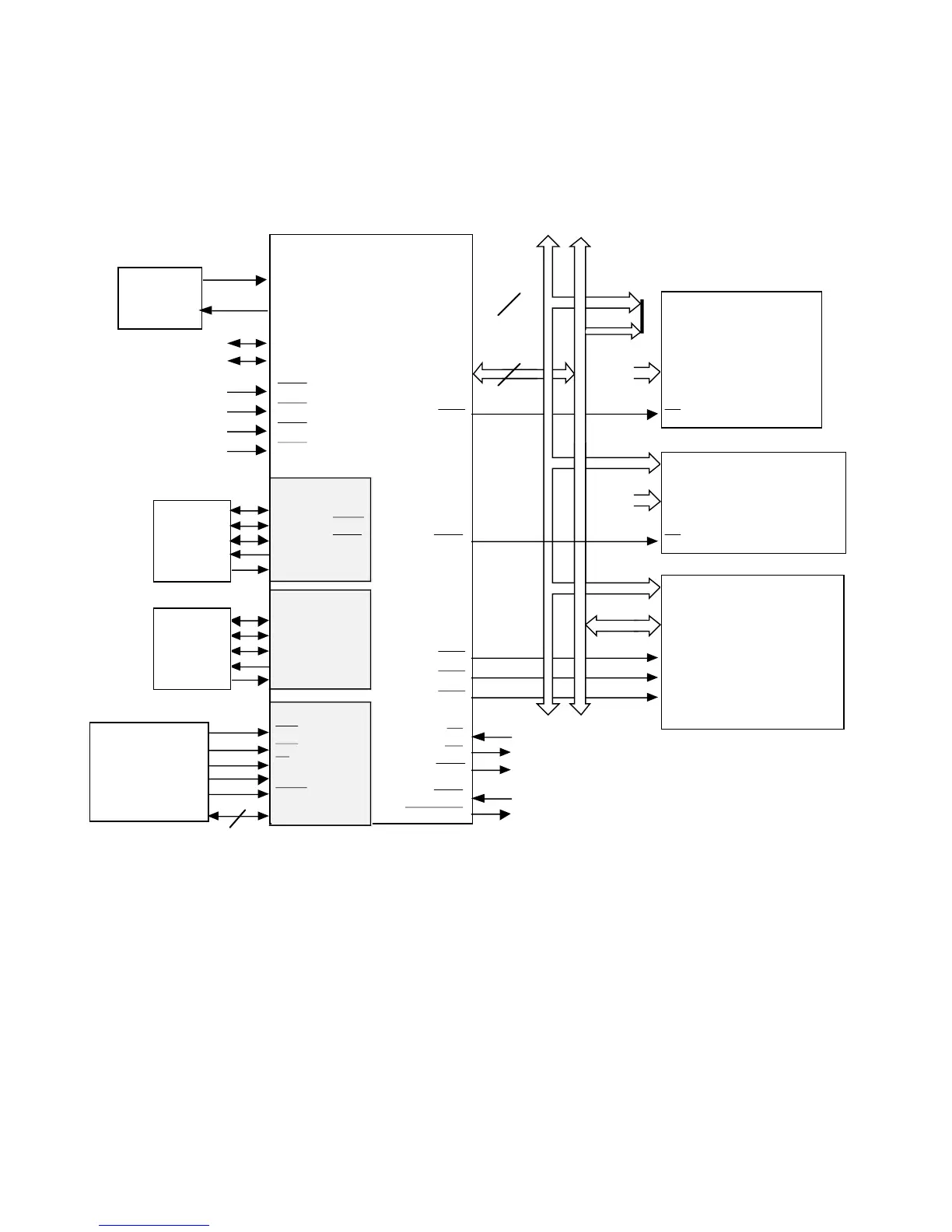
Figure 11.1 ADSP-2181 System
11.2 BDMA PORT
The ADSP-2181’s byte memory space is 8 bits wide and can address up to
4M bytes of program code or data. This memory space takes the place of
the boot memory space found on other ADSP-2100 family processors.
Unlike boot memory space, byte memory has read/write access through
the ADSP-2181’s BDMA port.
Each read/write to byte memory consists of data (on data bus lines 15:8)
and address (on address bus lines 13:0 plus data lines 23:16). The 22-bit
byte memory address lets you access up to 4M bytes of ROM or RAM.
BR
BG
CLKIN
IRQ2
ADSP-2181
1/2x CLOCK
or
CRYSTAL
XTAL
DR1
or
FI
SERIAL
DEVICE
DT1
or
FO
SCLK1
SPORT 1
RFS1
or
IRQ0
TFS1
or
IRQ1
DR0
DT0
TFS0
SCLK0
RFS0
SPORT 0
SERIAL
DEVICE
ADDR
DATA
PMS
DMS
ADDR
13-0
DATA
23-0
ADDR
DATA
A0-A21
DATA
CS
OVERLAY
MEMORY
Two 8K
PM Segments
Two 8K
DM Segments
I/O SPACE
(PERIPHERALS)
14
24
D
23-16
A
13-0
D
15-8
D
23-8
D
23-0
A
10-0
A
13-0
BMS
BYTE
MEMORY
2048 Locations
CSIOMS
CMS
IACK
IAL
IS
IRD
IWR
IDMA PORT
SYSTEM
INTERFACE
or
µCONTROLLER
16
IAD15-0
BGH
IRQE
IRQL0
IRQL1
PWD
PWDACK
PF0-7
FL0-2

 Loading...

