10Memory Interface
10 – 23
CLKOUT
xMS
RD
WR
BR
BG
BGH
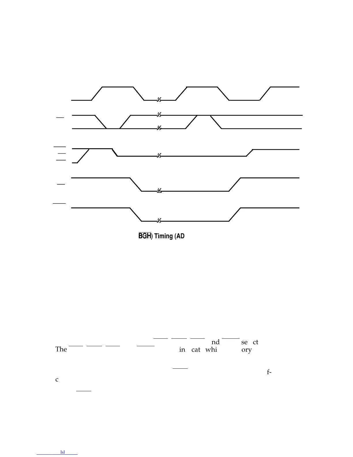
Figure 10.22 Bus Grant Hung (
BGHBGH
BGHBGH
BGH
) Timing (ADSP-2171, ADSP-2181 only)
10.6 ADSP-2181 MEMORY INTERFACES
The ADSP-2181 has the same modified Harvard architecture for internal
memory as the other processors of the ADSP-2100 family. In this
architecture, Data Memory stores data values and Program Memory
stores both instructions and data. The ADSP-2181 has as its full base
memory on-chip: 16K x 24-bit words of internal program memory RAM
and 16K x 16-bit words of internal data memory RAM.
There are four separate memory spaces: data memory, program memory,
byte memory, and I/O memory. To provide external access to these
memory spaces, the ADSP-2181 extends the internal address and data
buses off-chip and provides the
PMS
,
DMS
,
BMS
, and
IOMS
select lines.
The
PMS
,
DMS
,
BMS
, and
IOMS
signals indicate which memory space is
being accessed.
The composite memory space (and its
CMS
select line) lets a single off-
chip memory be accessed as multiple memory spaces. The Composite
Memory Select register lets you define which memory spaces are selected
by the
CMS
signal.

 Loading...

