10 Memory Interface
10 – 24
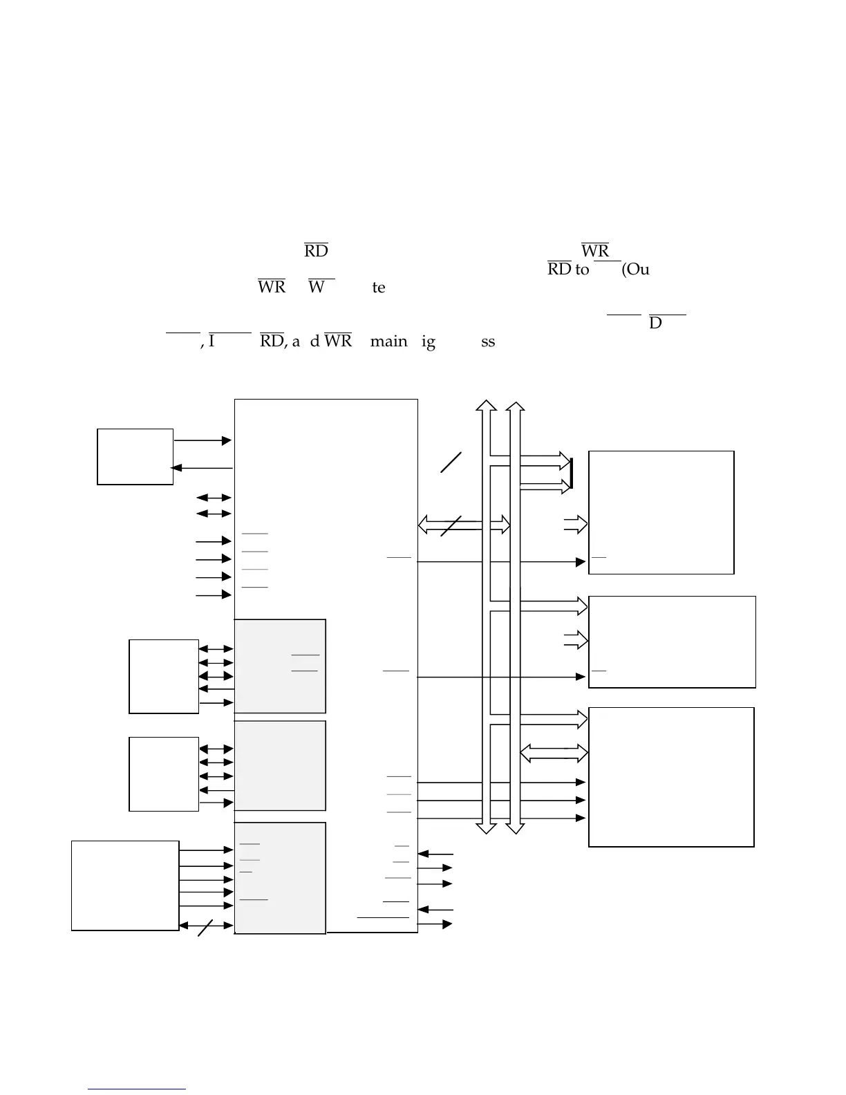
Figure 10.23 shows the external memory buses and control signals in an
ADSP-2181 system. Two control lines determine the direction of external
memory transfers:
RD
is active low signaling a read and
WR
is active low
for a write operation. Typically, you would connect
RD
to
OE
(Output
Enable) and
WR
to
WE
(Write Enable) of your memory.
Internal memory accesses do not drive any external signals:
PMS
,
DMS
,
BMS
,
IOMS
,
RD
, and
WR
remain high (deasserted), and the address and
data buses are tristated.
Figure 10.23 ADSP-2181 System Diagram
BR
BG
CLKIN
IRQ2
ADSP-2181
1/2x CLOCK
or
CRYSTAL
XTAL
DR1
or
FI
SERIAL
DEVICE
DT1
or
FO
SCLK1
SPORT 1
RFS1
or
IRQ0
TFS1
or
IRQ1
DR0
DT0
TFS0
SCLK0
RFS0
SPORT 0
SERIAL
DEVICE
ADDR
DATA
PMS
DMS
ADDR
13-0
DATA
23-0
ADDR
DATA
A0-A21
DATA
CS
OVERLAY
MEMORY
Two 8K
PM Segments
Two 8K
DM Segments
I/O SPACE
(PERIPHERALS)
14
24
D
23-16
A
13-0
D
15-8
D
23-8
D
23-0
A
10-0
A
13-0
BMS
BYTE
MEMORY
2048 Locations
CSIOMS
CMS
IACK
IAL
IS
IRD
IWR
IDMA PORT
SYSTEM
INTERFACE
or
µCONTROLLER
16
IAD15-0
BGH
IRQE
IRQL0
IRQL1
PWD
PWDACK
PF0-7
FL0-2

 Loading...

