7Host Interface Port
7 –
13
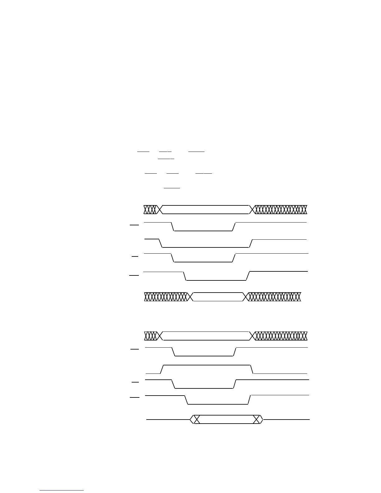
HMD0 selects separate read and write strobes, and HMD1 selects separate
address and data buses. The timing for the read cycle and the write cycle
is as follows:
1. The host asserts the address.
2. The host asserts (H
RD or HWR) and HSEL.
3. The ADSP-21xx returns HACK (and, for a read cycle, the data).
4. For a write cycle, the host asserts the data.
5. The host deasserts (H
RD or HWR) and HSEL.
6. The host deasserts the address (and, for a write cycle, the data).
7. The ADSP-21xx deasserts H
ACK (and, for a read cycle, the data).
Figure 7.7 shows the HIP timing when HMD0=1 and HMD1=0. HMD0
HD15–0 DATA
HSEL
HDS
HACK
HA2–0
ADDRESS
HRW
HSEL
HDS
HACK
HA2–0
ADDRESS
HRW
HD15–0 DATA
Host Write Cycle
Host Read Cycle
Figure 7.7 HIP Timing: Multiplexed R/W Strobe, Separate Buses

 Loading...

