11DMA Ports
11 – 19
IS
IAD15-0
IACK
IRD
PREVIOUS
DATA
READ
DATA
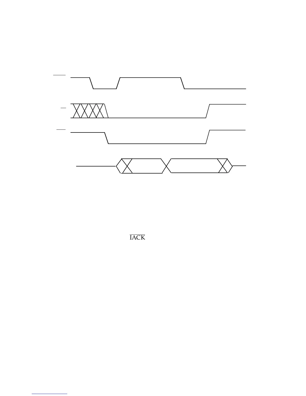
Figure 11.10 IDMA Long Read Cycle Timing
In the case of a Program Memory operation, the second IDMA port read
cycle for a given internal 24-bit word does not require an internal memory
access, does not wait for an instruction cycle boundary, and takes 1.5 or
2.5 cycles.
The best- and worst-case response times given above assume no system hold offs.
Hold offs for DMA transfers are defined in the section “DMA Cycle
Stealing, DMA Hold Offs, and
IACK
Acknowledge” at the end of this
chapter.
Warning: If an IDMA address latch cycle or an ADSP-2181 write to the
IDMA Control Register occurs after a first Program Memory read cycle (16
bits), the IDMA port will lose the second half of the Program Memory
word. The ADSP-2181 treats the next IDMA access as the first operation
for the new IDMA address and destination.

 Loading...

