4 Data Transfer
4 – 2
L
REGISTERS
4 x 14
MUX
ADDRESS
DMD BUS
FROM
INSTRUCTION
ADD
I
REGISTERS
4 x 14
M
REGISTERS
4 x 14
MODULUS
LOGIC
BIT
REVERSE
142 14 14 14
14
DAG1 ONLY
FROM
INSTRUCTION
2
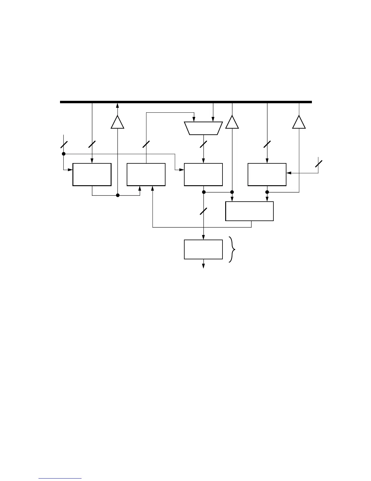
Figure 4.1 Data Address Generator Block Diagram
The I registers (I0-I3 in DAG1, I4-I7 in DAG2) contain the actual addresses
used to access memory. When data is accessed in indirect mode, the
address stored in the selected I register becomes the memory address.
With DAG1, the output address can be bit-reversed by setting the
appropriate mode bit in the mode status register (MSTAT) as discussed
below or by using the ENA BIT_REV instruction. Bit-reversal facilitates
FFT addressing.
The data address generators employ a post-modify scheme; after an
indirect data access, the specified M register (M0-M3 in DAG1, M4-M7 in
DAG2) is added to the specified I register to generate the updated I value.
The choice of the I and M registers are independent within each DAG. In
other words, any register in the I0-3 set may be modified by any register in
the M0-M3 set in any combination, but not by those in DAG2 (M4-M7).
The modification values stored in M registers are signed numbers so that
the next address can be either higher or lower.

 Loading...

