6.7 CC-Link Interface Card
6-159
Chap. 6
CONTROL OPTIONS
6.7.4 Basic connection diagram
Refer to "6.1.4 Installing internal options (OPC-VG1-)", and then perform wiring and connecting jobs.
・ Incorrect handling in connecting wires could cause an accident such as electric shock or fire. Qualified
electricians should carry out connecting wires. If connecting wires, for example, after the power is turned ON
requires any touching of an electric circuit, turn OFF (open) the breaker on the power supply side to prevent
electric shock.
・ Since the smoothing condenser has been charged although the breaker is turned OFF (open), touching of an
electric circuit causes an electric shock. Turn OFF the charge lamp (CHARGE) of the inverter, and confirm,
with a tester, etc., that the DC voltage of the inverter has been reduced to the safety voltage.
・ Do not use the product that is damaged or lacking parts. Doing so could cause injury or damage.
・ Incorrect handling in installation/removal could result in a broken product.
The basic connection diagram is shown below. When connecting the communications card, observe the
following precautions.
[Connecting precautions]
(1) Use dedicated cables (refer to 6.7.2.2 "Specifications") for CC-Link connection.
Be sure not to use soldered cables, which could cause disconnection or wire break.
(2) Use terminating registers that came with the PLC.
(3) For the maximum number of communications cards, refer to the number of units connectable in
6.7.2.2 "Specifications".
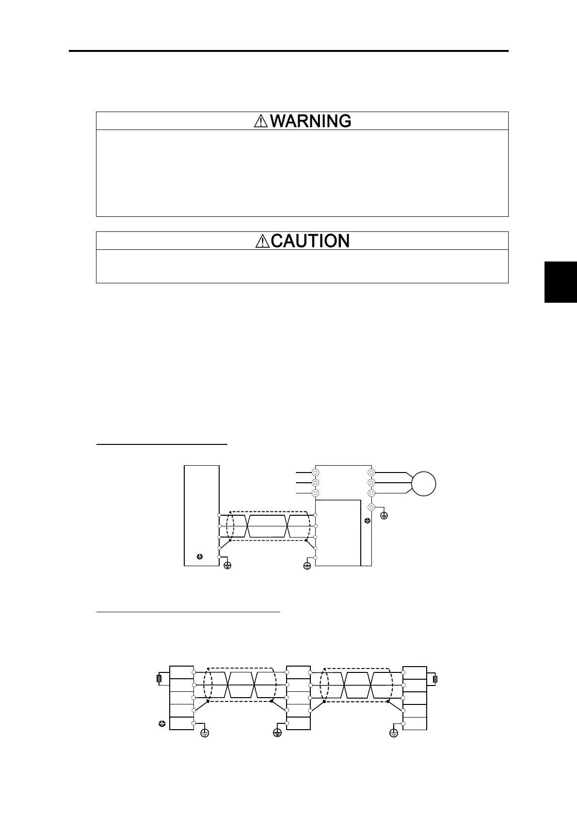
When an inverter is connected
CC-Link master FRENIC-VG
DA
DB
DG
SLD
U
V
W
R
S
T
Power supply
OPC-VG1-CCL
DA
DB
DG
SLD
G
M
3~
FG
CC-Link dedicated cable
FG
Figure 6.7.6 Inverter connection diagram (1 unit)
When two or more inverters are connected
For the number of inverters connectable, refer to Section 6.7.2.2 "Specifications."
CC-Link master
DA
DB
DG
SLD
CC-Link
dedicated cable
FG
DA
DB
DG
SLD
FG
FRENIC-VG invertor
OPC-VG1-CCL
CC-Link
dedicated cable
DA
DB
DG
SLD
FG
FRENIC-VG invertor
OPC-VG1-CCL
Terminating
register
Terminating
register
Figure 6.7.7 Inverter Connection Diagram (Two or More Inverters)
 Loading...