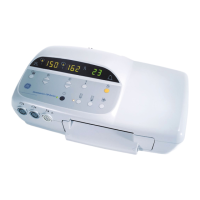
4-54 120 Series Maternal/Fetal Monitor Revision B
2015590-001
Theory of Operation: UA/FECG Board
The serial data from the A/D is transferred from the isolated circuitry to the
unisolated circuitry by the use of opto-isolators. The A/D clock and data are
buffered by gates in U15 which in turn drive the LED side of dual opto-isolator U14.
The restored clock and data on the output side of this isolator is sent to the DSP
Board where the data is converted to a parallel format that the processor can access.
The convert pulse used to start the A/D conversion is generated at the DSP Board.
This signal is transferred to the isolated circuitry by another dual opto-isolator U6.
The output from U6 is buffered by two stages of U15 before connecting to the R/C*
input of the A/D.
By using the serial clock generated in the A/D, additional data is clocked between
the isolated and unisolated circuitry using serial in/parallel out and parallel in/serial
out shift registers. On the isolated side, U7 is parallel loaded with mode enables
(FECG ENABLE*, TOCO EN*, etc) and other control signals when the R/C* line
of the A/D is driven low to start a conversion. The serial clock from the A/D
converter provides the clock signal for this part. As data is clocked from the A/D,
data is also shifted out of U7. The QH output from U7 drives the LED side of opto-
isolator U5, which transfers the serial data to the unisolated circuitry. While data is
being shifted from the A/D and from U7, serial data transferred from the unisolated
circuitry by opto-isolator U7 is clocked into U8, which also shares the common
serial clock. After the data has been shifted into the shift register section of U8, the
next convert pulse to the A/D will transfer the shift register outputs to the output
latch section of this part. The latched outputs of U8 provide control signals for the
option MECG board. On the unisolated side, shift register U19 is parallel loaded by
the DSP processor. The load pulse for U19 is decoded from a processor chip select
and write pulse by gate U23. The A/D serial clock, available through U14 on the
unisolated side is used to shift the data from U19 via opto-isolator U6 to U8 on the
isolated side. Only the lower four bits of the 8-bit byte are used by the isolated
circuitry. The upper four bits are retained on the unisolated side by latch U18,
which is loaded from the same decoded load pulse as U19. Two of these bits are
used on the unisolated side to control the selection of FET switch U17, and to
provide a control signal for the option MECG board to configure it for 50 or 60 Hz
operation. Data coming from U7 on the isolated side is clocked into shift registers
U20 and U21 using the common serial clock available to the unisolated circuitry.
As with U8, data is transferred from the shift register section of these parts to the
output latch section when a convert pulse is generated. The output latches are tri-
state and connect to the processor data bus. The output enable for these parts is
generated by decoding a chip select and read signal from the processor by a gate in
U23.
 Loading...