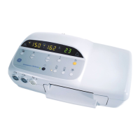
4-66 120 Series Maternal/Fetal Monitor Revision B
2015590-001
Theory of Operation: MECG Board
Test Generator
The test generator is composed of monostable U3 and an attenuation network
consisting of resistors R104–R110. U3, by the values of resistor R111 and capacitor
C54, is set to provide a 100 ms pulse every time it’s triggered from a control line
from the FECG/UA Board. When the input MUX is configured for the test
generator, the attenuated output of U3 connects to the input leads of the ECG
amplifier allowing for a board self test. The attenuation network scales the Q and
Q* outputs of U3 providing a 1 mV differential signal source. R106 offsets the Q*
output so that it is referenced to 0 V. R104 and R105 combine the right leg drive
output with the output of the generator. The logic supply for the test generator, as
well as all the other isolated logic is generated by an adjustable three-terminal
regulator VR1 from the isolated +15 V supply.
Linear Isolation Amplifier
All of the circuitry discussed so far has been electrically isolated from the main
system electronics. In order for the ECG output to get sampled and processed by the
main system, it must somehow get coupled over to the un-isolated circuitry without
effecting this electrical isolation. This is the function of linear opto-isolator U9. U9
consists of an LED and a pair of matched photodiodes. The LED is physically
located in the part to provide equal light intensity to both of the photodiodes. One
photodiode is used by the isolated circuitry, the other by the un-isolated. Since the
photodiodes are matched, current flowing through one will equal the current flowing
through the other, given the same supplies and load resistance. The isolation
amplifier relies on this to provide the needed signal path across the barrier. The
output from the last stage of the ECG amplifier is attenuated by two with resistors
R84 and R85. This is needed to keep the LED/photodiode pair within its linear
operating range. A stage of U6, along with current driver Q3, drives the LED
section of the opto-isolator with the divided input signal. C44 in the feedback of U6
limits the slew rate of the op-amp to prevent oscillations caused by feedback delays
associated with the opto-isolator. The anode of the LED connects to the emitter of
Q3 which can sink current to the + 15 V supply through its collector resistor R87,
and the cathode connects to the –15 V supply through R88. Feedback for U6 comes
from the output of the isolated photodiode through a 100 k
Ω resistor R101. The bias
for the photodiode/feedback resistor is supplied by ±10 V references. These are
generated by an inverting amplifier with a gain of two consisting of U12, R98–
R100, and C51 (–10 V) and by a non-inverting amplifier with a gain of two
consisting of another section of U12, R89–R90, and C47 (+10 V). The input used
by both these reference amplifiers is U16, a +5 V precision voltage reference. U6
and Q3 drive the LED with the input signal, and the feedback from the isolated
photodiode keeps the relationship between the input voltage and the current in both
photodiodes linear. The ±10 V references for the second photodiode are duplicated
on the un-isolated side with an inverting and non-inverting amplifier from two
stages of U8, and with U2 a second +5 V precision voltage reference. These
references connect across the un-isolated photodiode and a series output resistor that
duplicates the feedback configuration on the isolated side. The 100 k
Ω feedback
resistor however is replaced by the series combination of fixed resistor R114 and
potentiometer R115. This allows for the compensation of small current differences
and current transfer ratios between the two photodiodes. C56, in combination with
R114 and R115, is used to limit the high-frequency response of the isolator to under
800 Hz. The un-isolated photodiode output is buffered by a non-inverting amplifier
with a gain of two consisting of op-amp U8, and resistors R120 and R119. This
forms the final output stage of the isolation amplifier. The x2 gain is needed to