6-41
BUS INTERFACE UNIT
Also, bit 5 in the PINCFG register (Figure 5-15 on page 5-24) must be cleared, to connect the
coprocessor-related signals of the core to the package pins.
Below is an example of a simple routine that can be executed using the math-coprocessor:
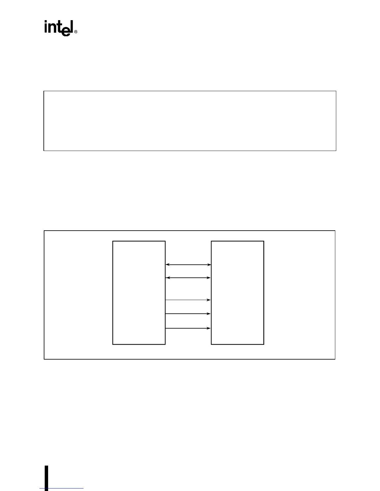
6.6.2 SRAM/FLASH Interface
SRAM and FLASH devices can be connected directly to the Intel386 EX processor as shown in
Figure 6-16. Separate CSn#, RD# and WR# strobes enable a “glueless” interface. The WR# sig-
nal, when used with an “EARLY READY#” (described in “Write Cycle” on page 6-16), guaran-
tees the ‘WE#-Inactive-to-Address-Invalid’ time of most SRAM and FLASH devices.
Figure 6-16. Intel386 EX Processor to SRAM/FLASH Interface
fninit ;; Initialize Math Coprocessor
fldpi ;; Load (Push on to the 387 stack) “Pi”
fld1 ;; Load (Push on to the 387 stack) “1”
fadd ;; Add the two values, i.e. Pi + 1
fist word ptr [di] ;; Convert to integer and Store at
;; location pointed to by DS:DI
Intel386™ EX
Embedded
Processor
OE#
CE#
WE#
A2853-02
SRAM
or FLASH
Address
Data
RD#
CS
n
#
WR#