112
Intel
®
855GME Chipset and Intel
®
6300ESB ICH Embedded Platform Design Guide
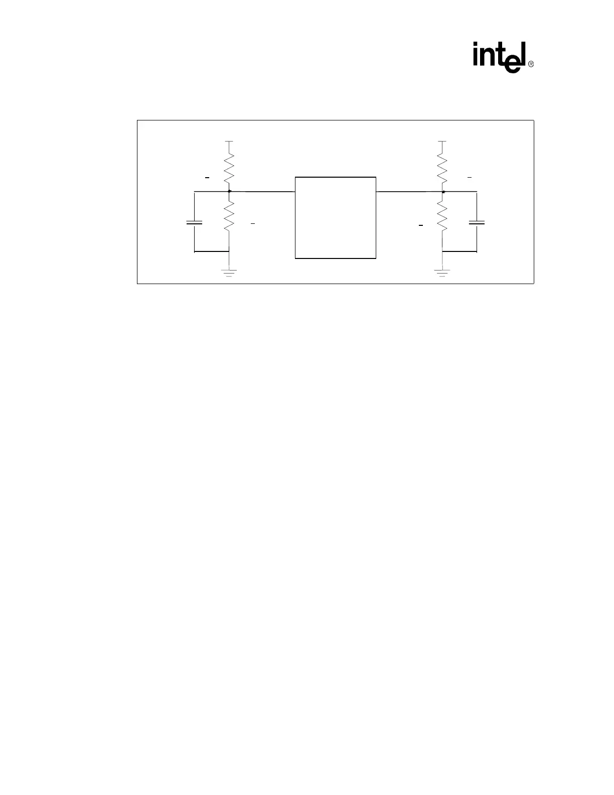
4.8.2.4 DDR VTT Termination
The recommended topology for DDR-SDRAM Data, Control, and Command signal groups
requires that all these signals be terminated to a 1.25 V source, VTT, at the end of the memory
channel opposite the GMCH. It is recommended that this VTT be generated from the same source
as used for VCCSM, and not be used for GMCH and DDR SMVREF. This is because SMVREF
has a much tighter tolerance and VTT may vary more easily depending on signal states. A solid
1.25 V termination island shall be used for this purpose and be placed on the surface signal layer,
just beyond the last DIMM connector and must be at least 50 mils wide.
The data and command signals shall be terminated using one resistor per signal. Resistor packs and
± 5 percent tolerant resistors are acceptable for this application. Only signals from the same DDR
signal group may share a resistor pack. Refer to Section 5 for system memory guidelines.
4.8.2.5 DDR SMRCOMP and VTT 1.25 V Supply Disable in S3/Suspend
Regardless of how these 1.25 V supplies for GMCH are generated, they may be disabled during the
S3 suspend state to further save power on the platform. This is possible because the GMCH does
not require the enabling of resistive compensation during suspend. However, some DDR memory
devices may require a valid reference voltage during suspend. It is the responsibility of the
system designer to ensure that requirements of the DDR memory devices are met.
Note: The 2.5 V VCCSM power pins of the GMCH and the VDD power pins of the DDR memory
devices do need to be on in S3 state.
Figure 54. GMCH System Memory Reference Voltage Generation Circuit
R1a
604
Ω
+1%
R2a
Ω
+VCCSM
855GME
Chipset
GMCH
SMVSWINGL
SMVSWINGL
SMVSWINGH
R1b
R2b
+VCCSM
0.1
μ
F 0.1
μ
F