January 2007 141
Intel
®
855GME Chipset and Intel
®
6300ESB ICH Embedded Platform Design Guide
System Memory Design Guidelines (DDR-SDRAM)
Length range formula for DIMM1:
X
1
= SCK[5:3]/SCK[5:3]# total reference length, including package length. Refer to
Section 5.4.3.1 for more information.
Y
1
= SCS[3:2]# and SCKE[3:2] total length = GMCH package length + L1, as shown in Figure 69,
where:
(X
1
– 1.5”) ≤ Y
1
≤ (X
1
- 0.5”)
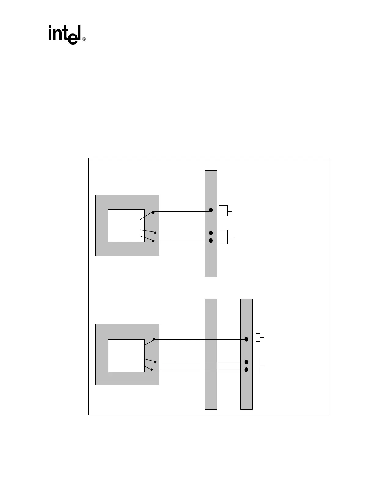
No length matching is required from the DIMM to the termination resistor. Figure 70 depicts the
length matching requirements between the control signals and clock. A nominal CS/CKE package
length of 500 mils may be used to estimate baseline Mbyte lengths.
Figure 70. Control Signal to Clock Trace Length Matching Diagram
GMCH Package
SCS#[1:0]
SCKE[1:0]
SCK[2:0]
SCK#[2:0]
ote: All lengths are measured from GMCH
ie pad to DIMM connector pads.
CTRL Length = Y0
Clock Ref. Length = X0
DIMM0 DIMM1
SCK[5:3]
SCK#[5:3]
Clock Ref. Length = X1
ote: All lengths are measured from GMCH
ie pad to DIMM connector pads.
SCS#[3:2]
SCKE[3:2]
CTRL Length = Y1
(X0 – 1.5" ) ≤ Y0 ≤ (X0 - 0.5")
(X1 – 1.5")
≤
Y1
≤
(X1- 0.5")
GMCH Package
855GME
Die
855GME
Die