January 2007 49
Intel
®
855GME Chipset and Intel
®
6300ESB ICH Embedded Platform Design Guide
Intel
®
Pentium
®
M/Celeron
®
M Processor FSB Design and Power Delivery Guidelines
Table 8 lists the source synchronous address signals general routing requirements. They should be
routed to a pin-to-pin length minimum of 0.50 inches and a maximum of 6.5 inches. Due to the
200 MHz, high-frequency operation of the address signals, the routing guidelines listed in Table 8
allow for 2:1 spacing for the address signals given a 55 Ω ± 15% characteristic trace impedance
except for address strobe signals. But if space permits, 3:1 spacing is strongly advised for these
signals.
4.1.3.3 Intel
®
Pentium
®
M/Celeron
®
M Processor and Intel
®
855GME Chipset
GMCH (82855GME) FSB Signal Package Lengths
Table 9 lists the preliminary package trace lengths of the Pentium M/Celeron M processor and the
82855GME for the source synchronous data and address signals. The Pentium M/Celeron M
processor FSB package signals within the same group are routed to the same package trace length,
but the Intel 855GME chipset package signals within the same group are not routed to the same
package trace length. As a result of this package length compensation is required for GMCH. Refer
to Section 4.1.4 for length matching constraints and to Section 4.1.4.1 package length
compensation for further details. The Pentium M/Celeron M processor package traces are routed as
micro-strip lines with a nominal characteristic impedance of 55 Ω ± 15 percent.
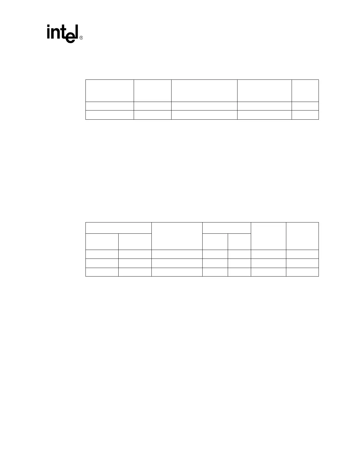
Table 7. Intel
®
Pentium
®
M/Celeron
®
M Processor FSB Address Source Synchronous
Signal Trace Length Mismatch Mapping
CPU Signal Name
Signal
Matching
Strobe Associated with the
Group
Strobe to Associated
Address Signal
Matching
Notes
REQ[4:0]#, A[16:3]# ± 200 mils ADSTB0# ± 200 mils 1, 2, 3
A[31:17]# ± 200 mils ADSTB1# ± 200 mils 1, 2, 3
NOTES:
1. ADSTB[1:0]# shall be trace length matched to the average length of the associated address signals group.
2. Each address signal shall be trace length matched to its associated address strobe within ± 200 mils.
3. All length matching formulas are based on GMCH die-pad to Pentium M/Celeron M processor pin total
length per signal group. Package length tables are provided for all signals to facilitate this pad to pin
matching.
Table 8. Intel
®
Pentium
®
M/Celeron
®
M Processor FSB Source Synchronous
Address Signal Routing Guidelines
Signal Names
Transmission Line
Type
Total Trace Length
Nominal
Impedance
(Ω)
Width and
Spacing
(mils)
Address
Group #1
Address
Group #2
Min
(inches)
Max
(inches)
A[16:3]# A[31:17]# Strip-line 0.50 6.5 55 ± 15% 4 and 8
REQ[4:0]# Strip-line 0.50 6.5 55 ± 15% 4 and 8
ADSTB#[0] ADSTB#[1] Strip-line 0.50 6.5 55 ± 15% 4 and 12