124
Intel
®
855GME Chipset and Intel
®
6300ESB ICH Embedded Platform Design Guide
System Memory Design Guidelines (DDR-SDRAM)
5.2 Length Matching and Length Formulas
The routing guidelines presented in the following subsections define the recommended routing
topologies, trace width and spacing geometries, and absolute minimum and maximum routed
lengths for each signal group, which are recommended to achieve optimal SI and timing. In
addition to the absolute length limits provided in the individual guideline tables, more restrictive
length matching formulas are also provided that further restrict the minimum to maximum length
range of each signal group with respect to clock, within the overall boundaries, as required to
ensure adequate timing margins. These secondary constraints are referred to as length matching
constraints and the formulas used are referred to as length matching formulas.
All signal groups, except feedback signals, are length matched to the DDR clocks. The clocks on a
given DIMM are matched to within ± 25 mils of the target length. A different clock target length
may be used for each DIMM. The difference in clock target lengths between DIMM0 and DIMM1
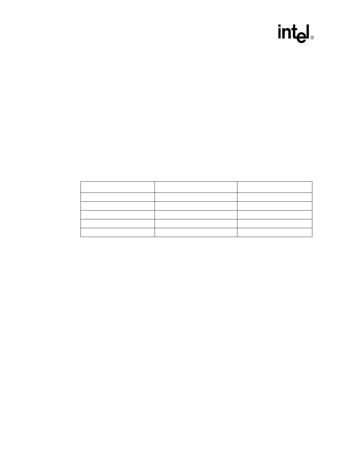
shall not exceed 1 inch. A simple summary of the length matching formulas for each signal group
is provided in Table 28.
Package length tables are provided for all signals to facilitate this pad-to-pin matching. Length
formulas shall be applied to each DIMM slot separately. The full geometry and routing guidelines
along with the exact length matching formulas and associated diagrams are provided in the
individual signal group guidelines sections to follow.
An available DDR DIMM trace length calculator may be used to ensure layout trace lengths meet
these recommendations. Contact the local Intel Field Representative for information on obtaining
this tool.
5.3 Package Length Compensation
As mentioned above, all length matching is done for GMCH die-pad to DIMM pin. The reason for
this is to compensate for the package length variation across each signal group in order. The Intel
855GME chipset Graphics Memory Controller Hub (82855GME) does not equalize package
lengths internally as some previous GMCH components have; the 82855GME requires length
matching or tuning process. The justification for this is based on the belief that length variance in
the package based on ball position is naturally tuned out when the pin escape is completed to the
edge of the package. Length matching in the package would then tend to create a mismatch at the
package edge.
Package length compensation shall not be confused with length matching as discussed in the
previous section. Length matching refers to constraints on the minimum and maximum length
bounds of a signal group based on clock length, whereas package length compensation refers to the
Table 28. Length Matching Formulas
Signal Group Minimum Length Maximum Length
Control to Clock Clock –1.5” Clock - 0.5”
Command to Clock Clock – 1.5” Clock + 1.0”
CPC to Clock Clock – 1.5” Clock - 0.5”
Strobe to Clock Clock – 1.5” Clock - 0.5”
Data to Strobe Strobe – 25 mils Strobe + 25 mils
NOTE: All length matching formulas are based on GMCH die-pad to DIMM pin total length.