EasyManua.ls Logo

Intel 855GME User Manual

Intel 855GME
320 pages
To Next Page IconTo Next Page
To Previous Page IconTo Previous Page
Page #180 background imageLoading...
Page #180 background image
180 Design Guide
Intel
®
855GME Chipset and Intel
®
82801DB ICH4 Embedded Platform Design Guide
AGP Port Design Guidelines
7.2.7 Pull-Ups
The AGP 2.0 Specification requires AGP control signals to have pull-up resistors to VDDQ to
ensure they contain stable values when no agent is actively driving the bus. Also, the
AD_STB[1:0]# and ST_STB# strobes require pull-down resistors to GND. The Intel 855GME
chipset GMCH has integrated many of these pull-up/pull-down resistors on the AGP interface and
a few other signals not required by the AGP 2.0 Specification. Pull-ups are allowed on any signal
except AD_STB[1:0]# and SB_STB#.
The Intel chipset GMCH has no support for the PERR# and SERR# pins of an AGP graphics
controller that supports PERR# and SERR#. Pull-ups to a 1.5-V source are required down on the
motherboard in such cases.
NOTES:
1. The Intel chipset GMCH has integrated pull-ups to ensure that these signals do not float when there is no
add-in card in the connector.
2. The Intel chipset GMCH does not implement the PERR# and SERR# signals. Pull-ups on the motherboard
are required for AGP graphics controllers that implement these signals.
3. The Intel chipset GMCH does not implement interrupt signals. AGP graphics controller's INTA# and INTB#
signals must but routed to the system PCI interrupt request handler where the pull-up requirement should be
met as well. For 855GME/ICH4 chipset-based systems, they can be routed to the ICH4's PIRQ signals that
are open drain and require pull-ups on the motherboard.
4. ST[1:0] provide the strapping options for 100-MHz PSB operation and DDR memory, respectively.
5. INTA# and INTB# should be pulled to 3.3 V, not VDDQ.
6. The pull-up/pull-down resistor value requirements are shown in Table 65.
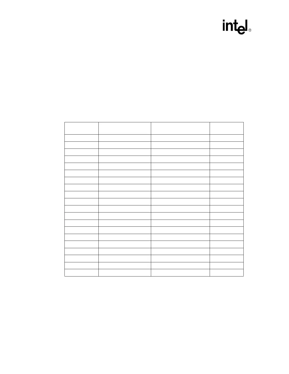
Table 64. AGP Pull-Up/Pull-Down Requirements and Straps
Signal
AGP 2.0 Signal Pull-Up/
Pull-Down Requirements
GMCH Integrated Pull-Up/
Pull-Down
Notes
DEVSEL# Pull-Up
FRAME# Pull-Up
GNT# Pull-Up
INTA# Pull-Up 3, 5
INTB# Pull-Up 3, 5
IRDY# Pull-Up
PERR# Pull-Up 2
PIPE# Pull-Up
RBF# Pull-Up
REQ# Pull-Up 1
SERR# Pull-Up 2
ST[2:0] Pull-Down 4
STOP# Pull-Up Pull-Up
TRDY# Pull-Up
WBF# Pull-Up
AD_STB[1:0] Pull-Up
AD_STB[1:0]# Pull-Down
SB_STB Pull-Up
SB_STB# Pull-Down
SBA[7:0] Pull-Up 1

Table of Contents

Question and Answer IconNeed help?

Do you have a question about the Intel 855GME and is the answer not in the manual?

Intel 855GME Specifications

General IconGeneral
ManufacturerIntel
Model855GME
TypeChipset
Graphics CoreIntel Extreme Graphics 2
Memory TypeDDR
Maximum Memory Size2 GB
FSB400MHz
Integrated VideoYes
Graphics Base Frequency200 MHz
PCI SupportYes
USB SupportUSB 2.0
ATA SupportATA-100
PackageMicro-FCBGA
Memory TypesDDR 200/266/333 MHz

Summary

3 General Design Considerations

4 Intel® Pentium® M/Celeron® M Processor FSB Design and Power Delivery Guidelines

4.1 Intel® Pentium® M/Celeron® M Processor FSB Design Recommendations

Provides recommendations for meeting timing and voltage specs for optimal operation.

4.4 Intel® Pentium® M/Celeron® M Processor Decoupling Recommendations

Offers guidelines for system board bulk and high-frequency decoupling capacitor solutions.

4.8 Intel 855GME Chipset Platform Power Delivery Guidelines

Provides guidelines for power delivery and decoupling for the Intel 855GME chipset.

5 System Memory Design Guidelines (DDR-SDRAM)

6 Integrated Graphics Display Port

7 AGP Port Design Guidelines

7.2 AGP Routing Guidelines

Provides routing guidelines for AGP 1X and 2X/4X timing domains.

8 Hub Interface

8.1 8-Bit Hub Interface Routing Guidelines.

Covers routing guidelines for 8-bit Hub Interface data and strobe signals.

9 Intel® 6300ESB Design Guidelines

9.6 USB 2.0

Covers layout guidelines for USB 2.0, including trace separation and connections.

9.10 PCI-X Design Guidelines

Provides guidelines for connecting and routing the 6300ESB PCI-X interface.

11 Platform Clock Routing Guidelines

11.2 Clock Group Topologies and Routing Constraints

Defines recommended topologies and rules for platform level clocks.

12 Schematic Checklist Summary

12.3 Intel® 855GME Chipset GMCH (82855GME) Checklist

Checklist for GMCH system memory interface and decoupling.

12.4 Intel® 6300ESB Checklist

Checklists for PCI-X, PCI, Hub, FWH/LPC, GPIO, USB, Power, CPU, System Management, RTC, UART, AC'97, Misc.

13 Layout Checklist

13.2 Intel® 855GME Chipset GMCH Layout Checklist

Layout checklist for GMCH interface signals and memory decoupling.

13.3 Intel® 6300ESB Layout Checklist

Provides layout guidelines for 8-bit Hub Interface, Serial ATA, IDE, USB 2.0, AC'97, RTC, PCI-X, PCI.

Related product manuals