January 2007 123
Intel
®
855GME Chipset and Intel
®
6300ESB ICH Embedded Platform Design Guide
System Memory Design Guidelines (DDR-SDRAM)
System Memory Design Guidelines
(DDR-SDRAM) 5
5.1 Introduction
The Intel
®
855GME Chipset Double Data Rate (DDR) SDRAM system memory interface consists
of SSTL-2 compatible signals. These SSTL-2 compatible signals have been divided into several
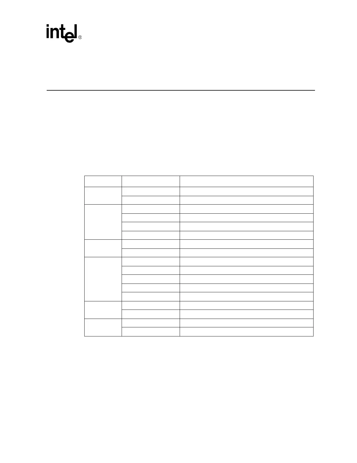
signal groups: data, control, command, CPC, clock, and feedback signals. Table 27 summarizes the
different signal grouping. Refer to the Intel
®
855GM/855GME Chipset Graphics and Memory
Controller Hub (GMCH) Datasheet for details on the signals listed.
Table 27. Intel
®
855GME Chipset DDR Signal Groups
Group Signal Name Description
Clocks
SCK[5:0] DDR-SDRAM differential clocks - (three per DIMM)
SCK[5:0]# DDR-SDRAM inverted differential clocks - (three per DIMM)
Data
SDQ[63:0] Data bus
SDQ[71:64] Check bits for ECC function
SDQS[8:0] Data strobes
SDM[8:0] Data mask
Control
SCKE[3:0] Clock enable - (one per Device Row)
SCS[3:0]# Chip select - (one per Device Row)
Command
SMA[12:6,3,0] Memory address bus
SBA [1:0] Bank select
SRAS# Row address select
SCAS# Column address select
SWE# Write enable
CPC
SMA[5,4,2,1] Command per clock (DIMM0)
SMAB[5,4,2,1] Command per clock (DIMM1)
Feedback
RCVENOUT# Receive enable output (no external connection)
RCVENIN# Receive enable input (no external connection)