140
Intel
®
855GME Chipset and Intel
®
6300ESB ICH Embedded Platform Design Guide
System Memory Design Guidelines (DDR-SDRAM)
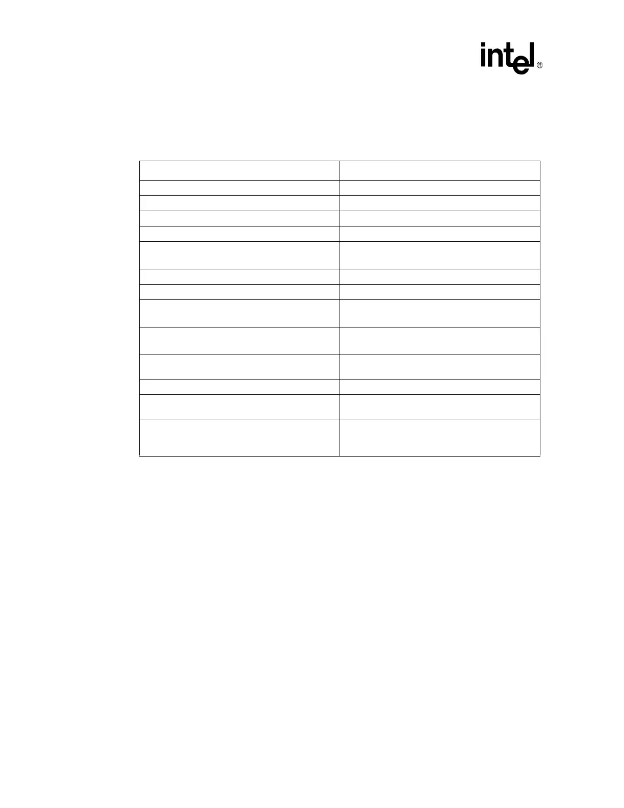
5.4.5.2 Control Signal Routing Guidelines
Table 36 defines the control signal routing guidelines.
5.4.5.3 Control to Clock Length Matching Requirements
The length of the control signals, between the GMCH die-pad and the DIMM must fall within the
range defined below, with respect to the associated clock reference length. Refer to Figure 69 for a
definition of the various trace segments that make up this path. The length of trace from the DIMM
to the termination resistor need not be length matched. The length matching requirements are also
shown in Figure 70.
Length range formula for DIMM0:
X
0
= SCK[2:0]/SCK[2:0]# total reference length, including package length. Refer to
Section 5.4.3.1 for more information.
Y
0
= SCS[1:0]# and SCKE[1:0] total length = GMCH package length + L1, as shown in Figure 69,
where:
(X
0
– 1.5”) ≤ Y
0
≤ (X
0
- 0.5”)
Table 36. Control Signal Routing Guidelines
Parameter Routing Guidelines
Signal Group SCKE[3:0], SCS[3:0]#
Motherboard Topology Point-to-Point with Parallel Termination
Reference Plane Ground Referenced
Characteristic Trace Impedance (Zo) 55
Ω ±15%
Nominal Trace Width
Inner layers: 4 mils
Outer layers: 5 mils
Minimum Spacing to Trace Width Ratio 2:1 (e.g., 8 mil space to 4 mil trace)
Minimum Isolation Spacing to non-DDR Signals 20 mils
Package Length P1
500 mils ± 250 mils
Refer to package length for exact lengths.
Trace Length P1 + L1 – GMCH Die-Pad to DIMM Pad
Min = 2.0 inches
Max = 6.0 inches
Trace Length L2 – DIMM Pad to Parallel Termination
Resistor Pad
Max = 2.0 inches
Parallel Termination Resistor (Rt) 56
Ω ±5%
Maximum Recommended Motherboard Via Count
Per Signal
3
Length Matching Requirements
Match CTRL to SCK[5:0]/SCK[5:0]#
Refer to length matching in Section 5.4.5.3 and
Figure 70.
NOTES:
1. Recommended resistor values and trace lengths may change in a later revision of the design guide.
2. Power distribution vias from Rt to Vtt are not included in this count.
3. It is possible to route using two vias if one via is shared that connects to the DIMM pad and parallel
termination resistor.
4. The overall maximum and minimum length to the DIMM must comply with clock length matching
requirements.