January 2007 187
Intel
®
855GME Chipset and Intel
®
6300ESB ICH Embedded Platform Design Guide
Hub Interface
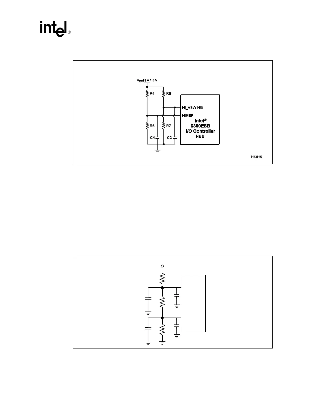
1. Each 0.01 µF bypass capacitor should be placed within 0.25 inches of HIREF/VREF pin (C4) and
HI_VSWING pin (C2).
8.1.4.1 GMCH Single Generated Voltage Reference Divider Circuit
This option allows the GMCH to use one voltage divider circuit to generate both HLVREF and
HLPSWING voltage references. The reference voltage for both HLVREF and HLPSWING must
meet the voltage specification in Table 68. The resistor values R1, R2, and R3 must be rated at 1
percent tolerance (see Table 69). Normal care needs to be taken to minimize crosstalk to other
signals (< 10-15 mV). When the voltage specifications are not met, individually generated voltage
divider circuits for HLVREF and PSWING are required. Refer to Section 8.1.4.2 for more details.
Figure 90 depicts the GMCH locally generated reference voltage divider circuit.
Figure 89. 8-Bit Hub Interface Local HIREF/HI_VSWING Generation Circuit Option D
Figure 90. GMCH Locally Generated Reference Voltage Divider Circuit
GMCH
HLVREF
R3
R2
C6
C5
PSWING
R1
1
3