186
Intel
®
855GME Chipset and Intel
®
6300ESB ICH Embedded Platform Design Guide
Hub Interface
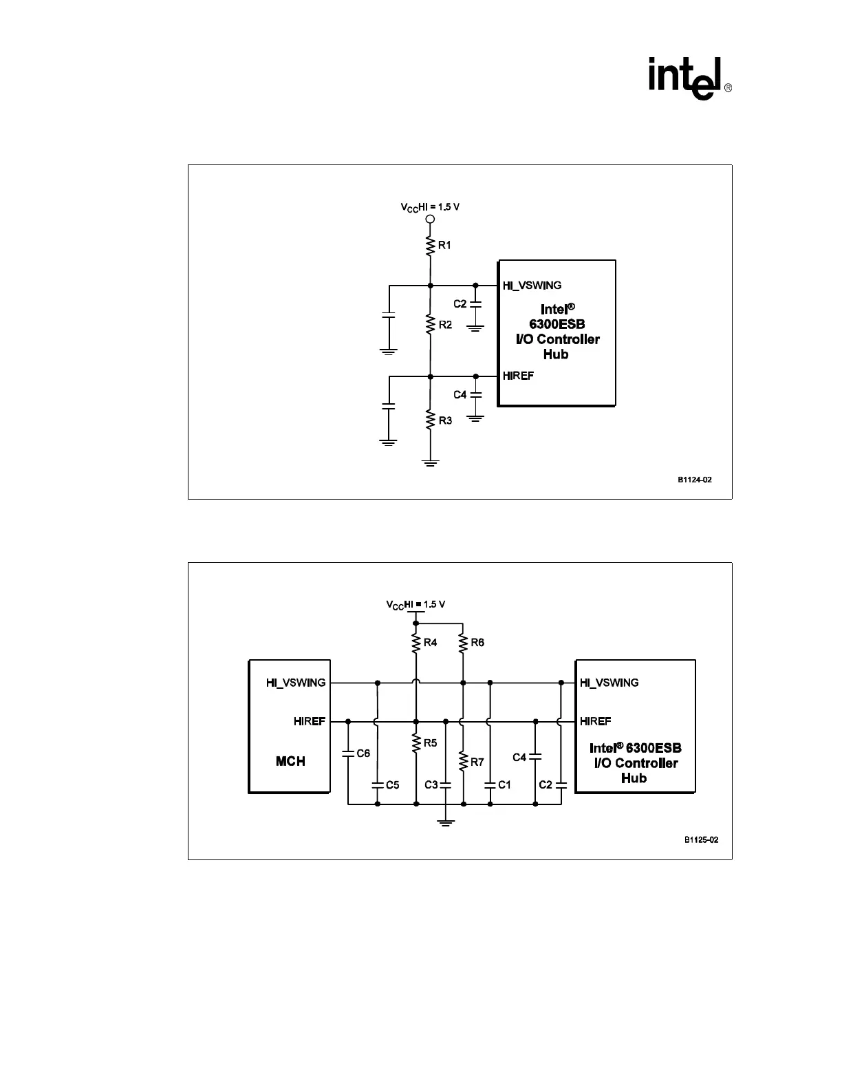
1. Each 0.01 µF bypass capacitor should be placed within 0.25 inches of HIREF/VREF pin (C4) and
HI_VSWING pin (C2).
1. Two 0.1 µF capacitors (C1 and C3) should be placed close to the divider.
2. Each 0.01 µF bypass capacitor (C2, C4, C5, and C6) should be placed within 0.25 inches of HIREF/VREF
pin (for C4 and C6) and HI_VSWING pin (for C2 and C5)
Figure 87. 8-Bit Hub Interface Local HIREF/HI_VSWING Generation Circuit Option B
Figure 88. 8-Bit Hub Interface Single HIREF/HI_VSWING Generation Circuit Option C