130
Intel
®
855GME Chipset and Intel
®
6300ESB ICH Embedded Platform Design Guide
System Memory Design Guidelines (DDR-SDRAM)
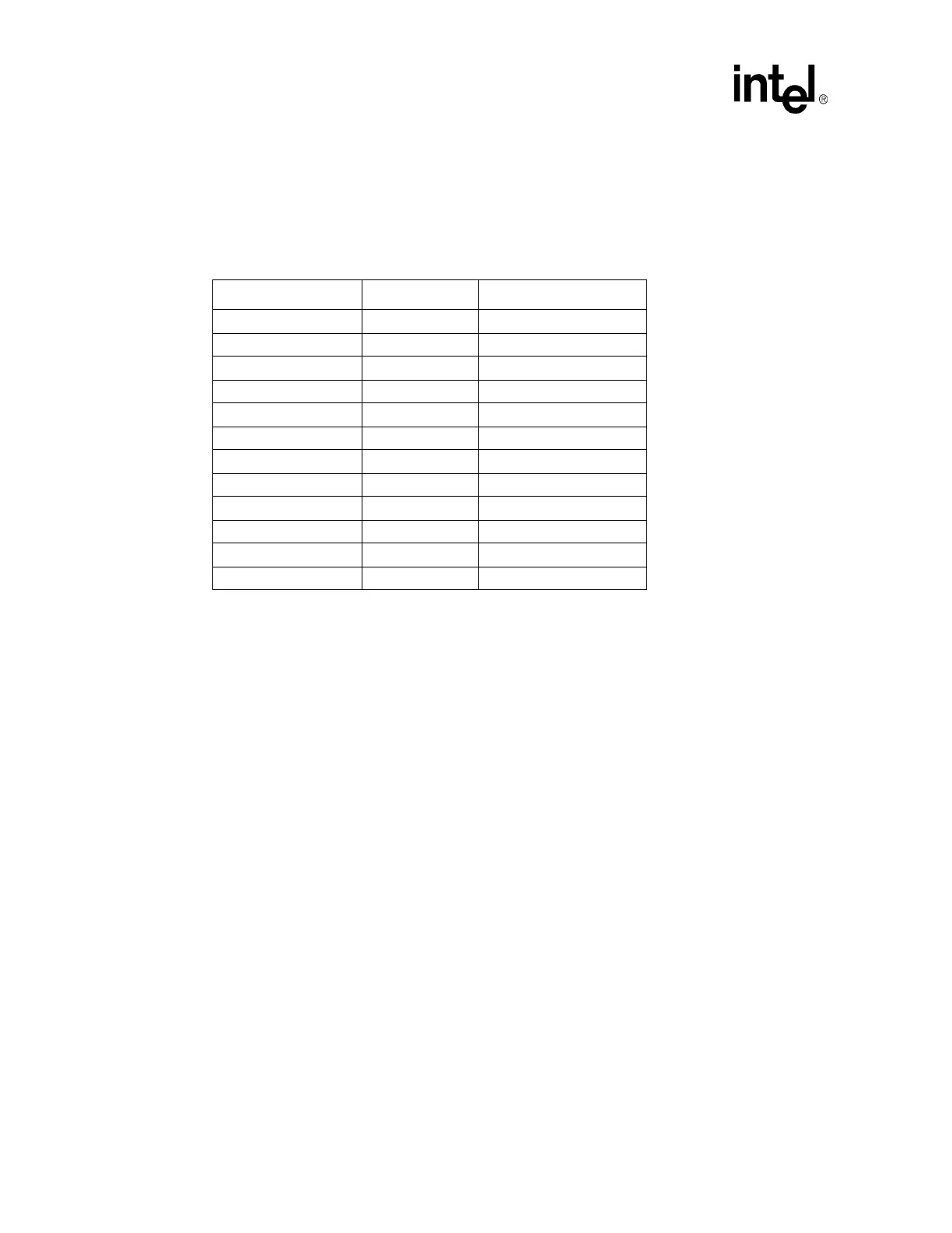
5.4.3.3 Clock Length Package Table
Use the package length data in Table 31 to tune the motherboard length of each SCK/SCK# clock
pair between the GMCH and the associated DIMM socket. Intel recommends that die-pad to
DIMM pin length be tuned to within ± 25 mils in order to optimize timing margins on the interface.
Package length compensation may be performed on each individual clock output thereby matching
total length on SCK/SCK# exactly, or alternatively the average package length may be used for
both outputs of a pair and length tuning done with respect to the motherboard portion only. See
Section 5.5.2 for more information on DRAM clock flexibility.
5.4.4 Data Signals – SDQ[71:0], SDM[8:0], SDQS[8:0]
The GMCH data signals are source synchronous signals that include a 72-bit wide data bus, a set of
eight data mask bits, and a set of eight data strobe signals. There is an associated data strobe and
data mask bit for each of the eight data byte groups, making for a total of eight 10-bit byte lanes.
This section summarizes the SDQ/SDM to SDQS routing guidelines and length matching
recommendations.
• The data signals include SDQ[71:0], SDM[8:0], and SDQS[8:0].
• The data signals shall transition from an external layer to an internal signal layer under the
GMCH. Keep to the same internal layer until transitioning back to an external layer at the
series resistor.
• After the series resistor, the signal shall transition from the external layer to the same internal
layer and route to DIMM0.
• At DIMM0, the signal shall transition to an external layer and connect to the appropriate pad
of the connector.
• After the DIMM0 transition, continue to route the signal on the same internal layer to DIMM1.
• Transition back out to an external layer and connect to the appropriate pad of DIMM1.
• Connection to the termination resistor shall be through the same internal layer with a transition
back to the external layer near the resistor. External trace lengths shall be minimized.
Table 31. DDR Clock Package Lengths
Signal Pin Number Package Length (mils)
SCK[0] AB2 1177
SCK[0]# AA2 1169
SCK[1] AC26 840
SCK[1]# AB25 838
SCK[2] AC3 1129
SCK[2]# AD4 1107
SCK[3] AC2 1299
SCK[3]# AD2 1305
SCK[4] AB23 643
SCK[4]# AB24 656
SCK[5] AA3 1128
SCK[5]# AB4 1146