January 2007 129
Intel
®
855GME Chipset and Intel
®
6300ESB ICH Embedded Platform Design Guide
System Memory Design Guidelines (DDR-SDRAM)
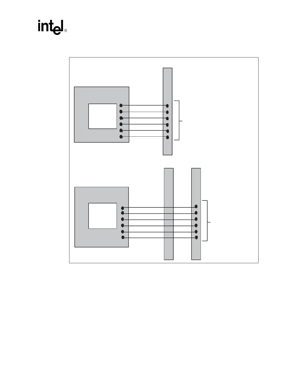
Figure 65. DDR Clock Trace Length Matching Diagram
DIMM0
Note: All lengths are measured from GMCH die -pad to
DIMM0 connector pads.
SCK0
SCK#0
SCK1
SCK#1
SCK0 Length = X0
SCK#0 Length = X0
SCK1 Length = X0
SCK#1 Length = X0
SCK3 Length = X1
SCK#3 Length = X1
SCK4 Length = X1
SCK#4 Length = X1
DIMM
0
DIMM
1
SCK3
SCK3#
SCK4
SCK4#
GMCH Package
Note: All lengths are measured from GMCH die - pad to
DIMM1 connector pads.
GMCH Package
Length = X0 ± 25 mils
(SCK to SCK# length ±10 mils)
Length = X1 ±25 mils
(SCK to SCK# length ±10 mils)
Clock Reference Length X0 =
_
_______
_
Clock Reference Length X1 =
__________
Intel
®
855GME
Chipset
Die
Die
AB2
AA2
AB25
AC26
AC2
AD2
AB23
AB24
SCK2
AC3
SCK#2
AD4
SCK2 Length = X0
SCK#2 Length = X0
SCK5
AA3
SCK#5
AB4
SCK5 Length = X1
SCK#5 Length = X1
Intel
®
855GME
Chipset