January 2007 65
Intel
®
855GME Chipset and Intel
®
6300ESB ICH Embedded Platform Design Guide
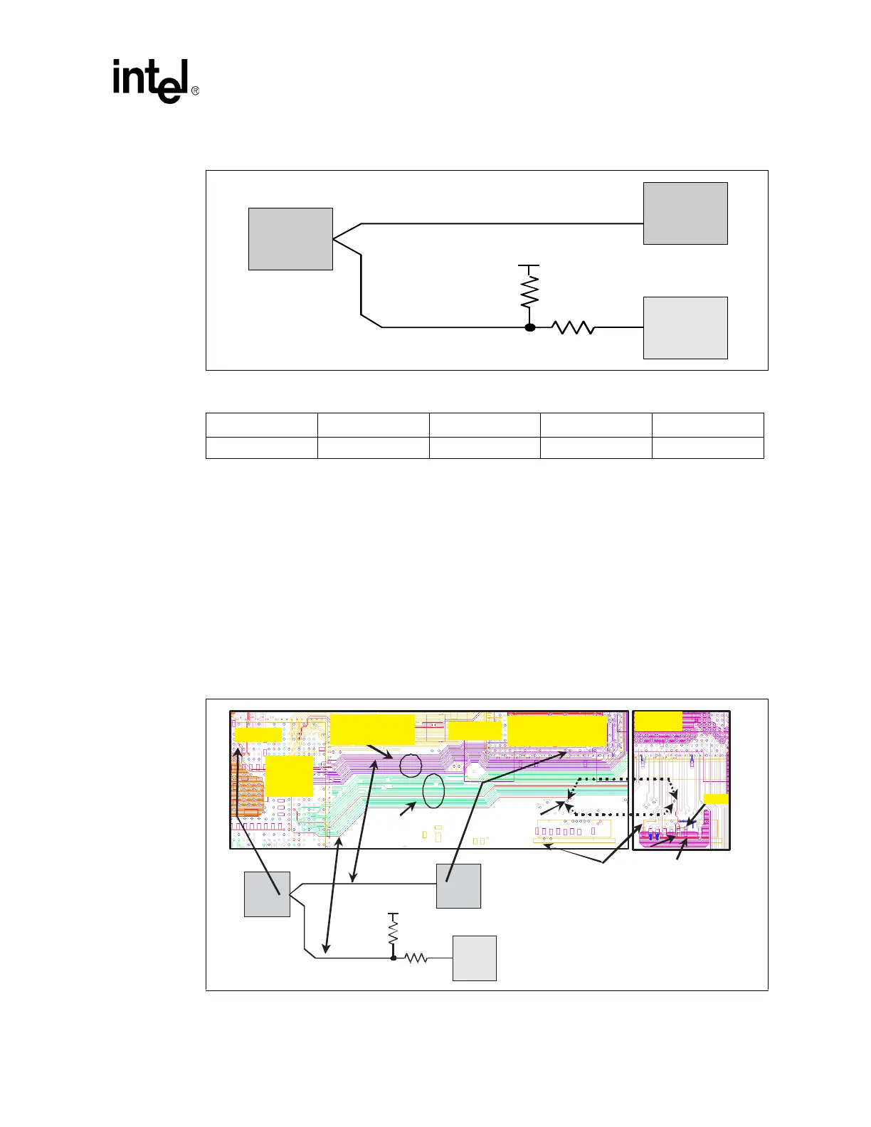
4.1.6.1 Processor RESET# Routing Example
Figure 25 illustrates a board routing example for the RESET# signal with an ITP700FLEX debug
port implemented. Figure 25 illustrates how the CPURST# pin of GMCH forks out into two
branches on Layer 6 of the motherboard. One branch is routed directly to the Intel Pentium
M/Celeron M processor RESET# pin among the rest of the common clock signals. Another branch
routes below the address signals and vias down to the secondary side that route to the Rs and Rtt
resistors. These resistors are placed in the vicinity of the ITP700FLEX debug port.
Note: The placement of Rs and Rtt next to each other is to minimize the routing between Rs and Rtt as
well as the minimal routing between Rs and the ITP700FLEX connector. Also, because a transition
between Layer 6 and the secondary side occurs, a GND stitching via is added to ensure continuous
ground reference of the secondary side routing of the RESET# signal to ITP700FLEX connector.
Figure 24. Processor RESET# Signal Routing Topology With ITP700FLEX Connector
Table 17. Processor RESET# Signal Routing Guidelines with ITP700FLEX Connector
L1 L2 + L3 L3 Rs Rtt
1.0” – 6.0” 6.0” max 0.5” max Rs = 22.6 Ω ± 1% Rtt = 220 ± 5%
CPU
L2
L3
Rs
L1
IT PF LEX
CONNECTOR
GMCH
Rtt
VCCP
RESET#
CPURESET#
RESET#
Figure 25. Processor RESET# Signal Routing Example with ITP700FLEX Debug Port
GND
CPU
L2
L3
Rs
L1
ITPFLEX
CONNECTOR
GMCH -
Rtt
VCCP
RESET#
CPURESET#
RESET#
Secondary
Side
Intel
®
Pentium
®
M
Processor
Intel
®
855GME
Chipset
ADDR
connector
Rs
VCCP
VIA
ITPFLEX
Layer 6
COMMON
Clock Signals
FORK
Rtt