January 2007 169
Intel
®
855GME Chipset and Intel
®
6300ESB ICH Embedded Platform Design Guide
Integrated Graphics Display Port
All signals shall be routed as striplines (inner layers).All signals in a signal group shall be routed on
the same layer. Routing studies have shown that these guidelines may be met. The trace length and
trace spacing requirements
must not be violated by any signal. Trace length mismatch for all
signals within a signal group shall be as close to ± 100 mils with respect to the strobe clocks as
possible to provide optimal timing margin. Table 55 depicts DVO enabled routing guideline
summary.
For DVO module case, the simulation model is the same as Figure 80 and the routing guideline is
the same as in Table 55; each strobe pair must be separated from other signals by at least 12 mils.
For multiplexed design, more conservative length mismatch (± 0.1 inches) is adopted.
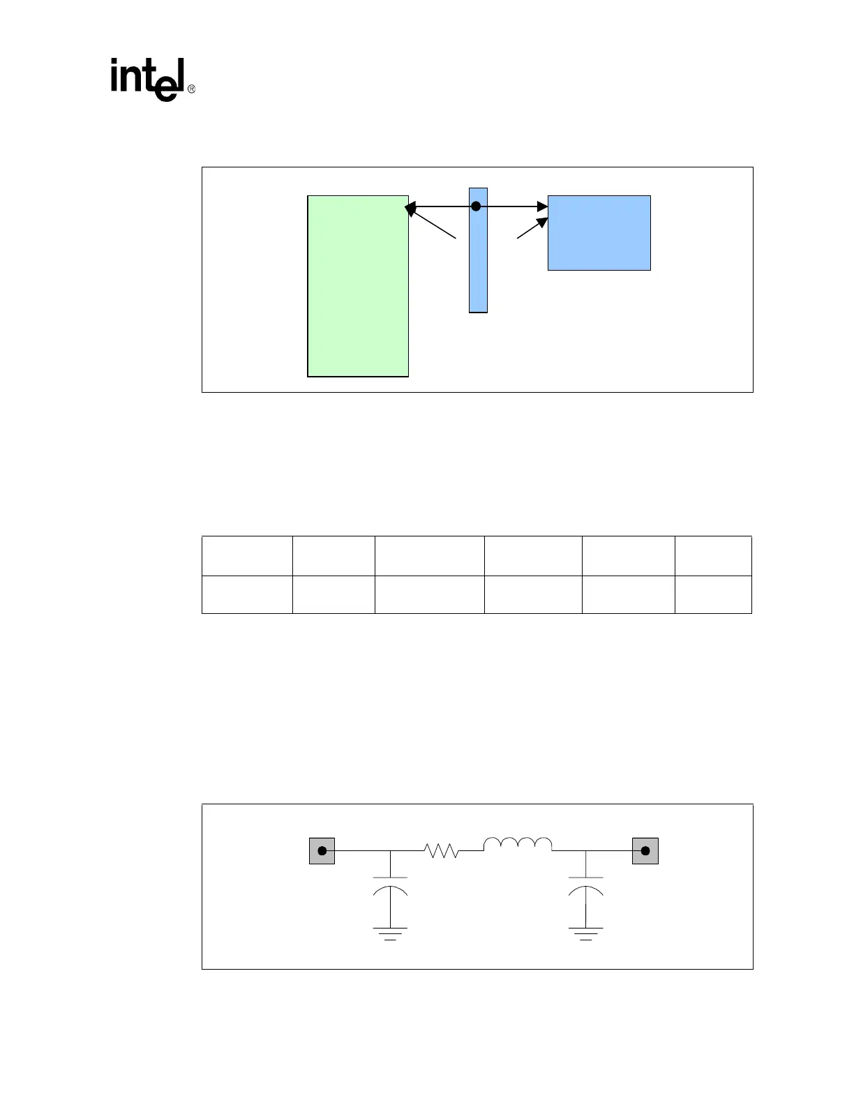
6.4.1.1 Generic Connector Model
Figure 81 depicts the generic connector model used in simulation for flexible DVO
implementation. This is only for reference. The actual connector may have different parasitic
values. Designs using this approach need to be simulated first.
Figure 80. DVO Enabled Simulation Model
DVOB &
DVOC I/F
Generic
Connector
GMCH
with
DVO
tDVb, tDVa
tDSu, tDh
tDVb, tDVa,
tDSu, tDh
L1
L2
Table 55. DVO Enabled Routing Guideline Summary
Signal
Maximum
Length
Trace Width Trace Spacing
Length
Mismatch
Notes
DVO Timing
Domain
L1=4 in
L2=2 in
4 mils 8 mils ± 100 mils
Figure 81. Generic Module Connector Parasitic Model
Motherboard Module
2.21 pF
C
2
2.21 pFC
1
2.5nH
RL
20mΩ