126
Intel
®
855GME Chipset and Intel
®
6300ESB ICH Embedded Platform Design Guide
System Memory Design Guidelines (DDR-SDRAM)
5.4.3 DDR Clock Routing Guidelines
Table 30 presents the DDR clock signal group routing guidelines.
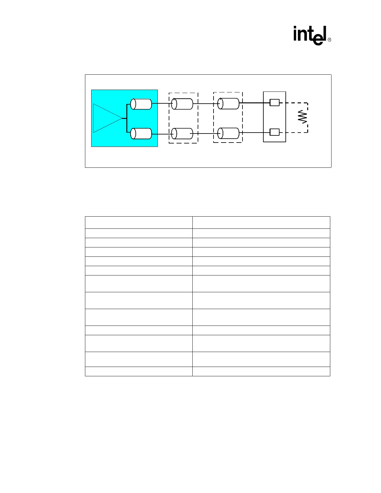
Figure 64. DDR Clock Routing Topology (SCK[5:0]/SCK[5:0]#)
NOTE: R1 is located on the DIMM module.
DIMM PADS
Differential Pairs
GMCH
R1
GMCH
Pin
P1
P1
L2
L2
L1
L1
Table 30. DDR Clock Signal Group Routing Guidelines (Sheet 1 of 2)
Parameter Definition
Signal Group SCK[5:0] and SCK[5:0]#
Topology Differential Pair Point to Point
Reference Plane Ground Referenced
Single Ended Trace Impedance (Zo) 42
Ω ±15%
Differential Mode Impedance (Zdiff) 70
Ω ±15%
Nominal Trace Width
(See exceptions for breakout region below.)
Inner Layers: 7 mils
Outer Layers: 8 mils (pin escapes only)
Nominal Pair Spacing (edge to edge)
(See exceptions for breakout region below)
Inner Layers: 4 mils
Outer Layers: 5 mils (pin escapes only)
Minimum Pair-to-Pair Spacing
(See exceptions for breakout region below.)
20 mils
Minimum Serpentine Spacing 20 mils
Minimum Spacing to Other DDR Signals
(See exceptions for breakout region below.)
20 mils
Minimum Isolation Spacing to Non-DDR
Signals
25 mils
Maximum Via Count 2 (per side)
NOTES:
1. Pad-to-pin length tuning is used on clocks to achieve minimal variance. Package lengths range between
approximately 600 mils and 1400 mils. Exact package lengths for each clock signal are provided at the
end of this section. Overall target length shall be established based on placement and routing flow. The
resulting motherboard segment lengths must fall within the ranges specified.
2. The DDR clocks shall be routed on internal layers, except for pin escapes. It is recommended that pin
escape vias be located directly adjacent to the ball pads on all clocks. Surface layer routing shall be
minimized.
3. Exceptions to the trace width and spacing geometries are allowed in the breakout region to fan-out the
interconnect pattern. Reduced spacing shall be avoided as much as possible.