January 2007 281
Intel
®
855GME Chipset and Intel
®
6300ESB ICH Embedded Platform Design Guide
Schematic Checklist Summary
12.3.5 Miscellaneous Signal Checklist
Table 129 presents the Miscellaneous signal checklist.
12.3.5.1 Intel
®
Pentium
®
M/Celeron
®
M Processor GST[2:0] Configurations
Table 130 presents the Intel Pentium M/Celeron M processor GST[2:0] configurations.
12.3.6 GMCH Decoupling Recommendations Checklist
Table 131 presents the GMCH decoupling recommendations checklist.
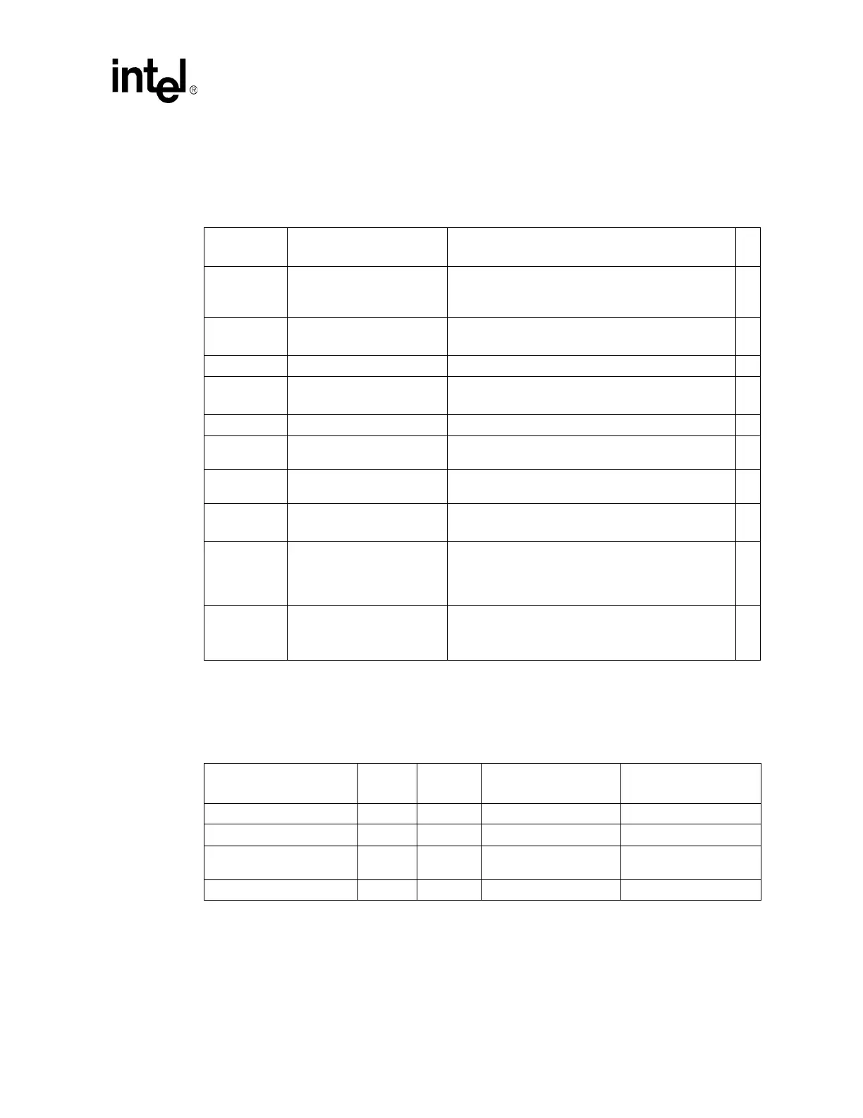
Table 129. Miscellaneous Signal Checklist
Pin Name
System
Pull-up/Pull-down
Notes
√
RSTIN#
Reset: (I)
Connect to the 6300ESB PCI_RST# pin (if ~4 loads).
May need to be buffered.
PWROK
Power OK: (I)
3 V signal. Indicates GMCH power is stable.
AGPBUSY# 8.2k pull-up to VCC3 AGP Busy: (O)
DDCACLK,
DDCADATA
2.2k pull-up to Vcc5 after
translation logic
CRT DDC Clock/Data
Needs to be translated from 3 V to 5 V.
EXTTS_0 10 K
Ω 1% pull-up to VCC3
LCLKCTLB
Used for SSC chip data control on Intel CRB. Leave this
signal as NC if not used.
LCLKCTLA
Used for SSC chip data control on Intel CRB. Leave as
NC if not used.
DREFCLK 33 ohm series at CK409.
DAC Display Clock Input
Connect to CK409 48 MHz DOT CLK (pin 38).
DREFSSCLK 33 ohm series at CK409.
LVDS SSC Clock Input. 48 MHz or 66 MHz, SSC or
non-SSC.
Connect to CK409 3V66_1/VCH CLK (pin 35). Optional
to connect to SSC chip for enhanced spread.
GST2 (C2)
GST1 (C3)
GST0 (C4)
Leave as NC or 1 K
Ω pull-up
to V_1P5_CORE
These pins have internal pull-down. Refer to Table 130
for GST[2:0] configuration options.
Table 130. GST[2:0] Configurations
Pentium
®
M Processor
GST[2:0] Configuration
FSB DDR Gfx Core Clock Low Gfx Core Clock High
000 400 266 133 200
001 400 200 100 200
010
(UXGA for 855GME only)
400 200 100 133
111 (855GME only) 400 333 166 250