34
Intel
®
855GME Chipset and Intel
®
6300ESB ICH Embedded Platform Design Guide
General Design Considerations
To meet the nominal 55 Ω characteristic impedance primary and secondary side layer micro-strip
lines are drawn at 5 mil trace width but end up with a 4 mil final trace width after etching. For the
same reason, the 5 mil thick prepreg between the primary side layer and Layer 2 starts at 5 mils but
becomes 4.5 mils after lamination. This situation and result also applies to Layer 7 and the
secondary side layer.
To ensure impedance control of 55 Ω, the primary and secondary side layer micro-strip lines shall
reference solid ground planes on Layer 2 and Layer 7, respectively.
Internal signal traces on Layer 3 and Layer 6 are unbalanced strip-lines. To meet the nominal 55 Ω
characteristic impedance for these traces, they reference a solid ground plane on Layer 2 and Layer
7. Because the coupling to Layer 4 and Layer 5 is still significant, (especially true when thinner
stack-ups use balanced strip-lines on internal layers) these layers are converted to ground floods in
the areas of the motherboard where the speed-critical interfaces such as the Intel Pentium
M/Celeron M Processor FSB or DDR system memory are routed. In the remaining sections of the
motherboard layout the Layer 4 and Layer 5 layers are used for power delivery.
For 55 Ω characteristic impedance Layer 3 (Layer 6), strip-lines have a 4 mil final trace width and
are separated by a core dielectric thickness of 4.8 mils after lamination from the Layer 2 (Layer 7)
ground plane and 4.8 mil thickness prepreg after lamination to separate it from Layer 4 (Layer 5).
The starting thickness of these core and prepreg dielectric layers before lamination is 5 mils and 5
mils, respectively.
The secondary side layer (L8) is also used for power delivery in many cases since it benefits from
the thick copper plating of the external layer plating as well as referencing the close (3 mil prepreg
thickness) Layer 7 ground plane. The benefit of such a stack-up is low inductance power delivery.
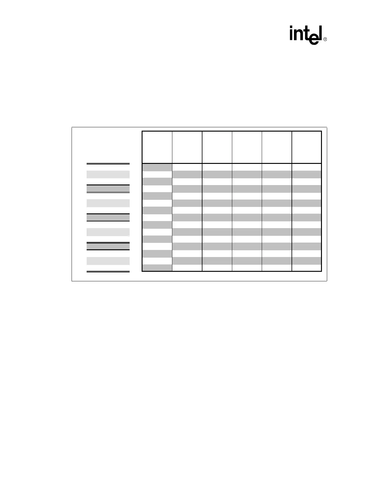
Figure 2. Recommended Board Stack-up Dimensions
Dielectric Layer Layer Copper Trace Trace
Thickness No. Type Weight Width Impedance
S
1 SIGNAL 1/2+plating 5 55
>3
P2PLANE1
>5
S3SIGNAL1455
>5
P4PLANE1
>28
P5PLANE1
>5
S6SIGNAL1455
>5
P7PLANE1
>3
8 SIGNAL 1/2+plating 5 55
S
(oz) (mils) (ohms)
CORE
PREPREG
(mills)
CORE
Stackup
PREPREG
PREPREG
PREPREG