January 2007 131
Intel
®
855GME Chipset and Intel
®
6300ESB ICH Embedded Platform Design Guide
System Memory Design Guidelines (DDR-SDRAM)
To facilitate routing, swapping of the byte lanes is allowed for SDQ[63:0]. Bit swapping within the
byte lane is also allowed for SDQ[63:0] only. The checkbits SDQ[71:64] cannot be byte lane
swapped with another SDQ byte lane. Bit swapping within the SDQ[71:64] byte lane is not
allowed. It is suggested that the parallel termination be placed on both sides of DIMM1 to simplify
routing and minimize trace lengths. All internal and external signals shall be ground referenced to
keep the path of the return current continuous.
Resistor packs are acceptable for the series (Rs) and parallel (Rt) data and strobe termination
resistors, but data and strobe signals cannot be placed within the same R pack as the command or
control signals. The tables and diagrams below depict the recommended topology and layout
routing guidelines for the DDR-SDRAM data signals.
Intel recommends that the full data bus SDQ[63:0], mask bus SDM[7:0], and strobe signals
SDQS[7:0] be routed on the same internal signal layer. It is required that the SDQ byte group and
the associated SDM and SDQS signals within a byte lane be routed on the same internal layer.
The total length of SDQ, SDM, and SDQS traces between the GMCH and the DIMMs must be
within the range defined in the overall guidelines, and is also constrained by a length range
boundary based on SCK/SCK# clock length, and an SDQ/SDM to SDQS length matching
requirement within each byte lane.
Note: All length matching must be done inclusive of package length. SDQ, SDM, and SDQS package
lengths are provided in Table 34 to facilitate this process.
There are two levels of matching implemented on the data bus signals. The first is the length range
constraint on the SDQS signals based on clock reference length. The second is SDQ/SDM to
SDQS length matching within a byte lane. The length of the SDQS signal for each byte lane must
fall within a range determined by the clock reference length, as defined in the SDQS to SCK/SCK#
length matching section. The actual length of SDQS for each byte lane may fall anywhere within
this range based on placement and routing flow.
After the SDQS length for a byte lane is established, the SDQ, SDM, and SDQS signals within the
byte lane must be length matched to each other, inclusive of package length, as described in the
SDQ to SDQS length matching section.
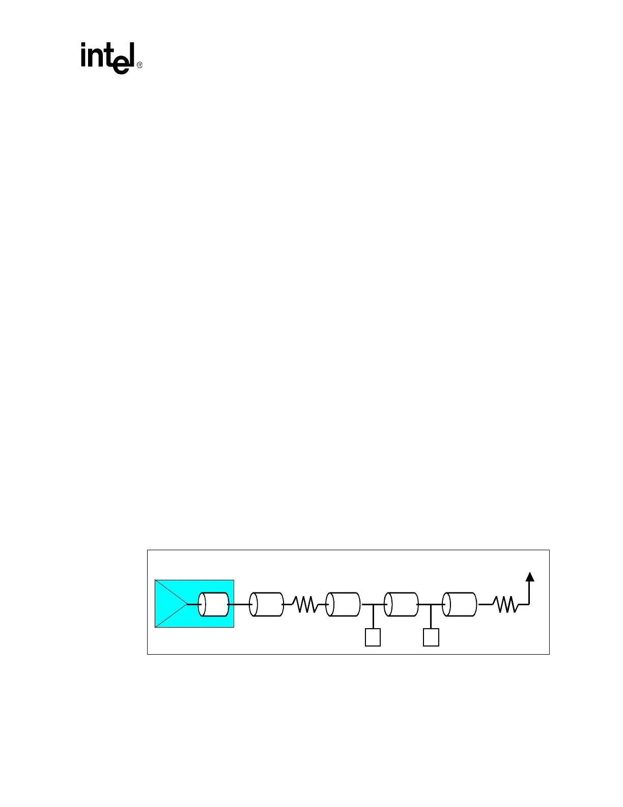
5.4.4.1 Data Bus Topology
Figure 66 depicts the data signal routing topology.
The data signals shall be routed using a 2:1 trace spacing to trace width ratio for signals within the
DDR group, except for clocks and strobes. Data signals shall be routed on inner layers with
minimized external trace lengths.
Figure 66. Data Signal Routing Topology
Rt
DIMM1 PAD
DIMM0 PAD
V
P1
L1
Die
L2
L3
L4
Rs