132
Intel
®
855GME Chipset and Intel
®
6300ESB ICH Embedded Platform Design Guide
System Memory Design Guidelines (DDR-SDRAM)
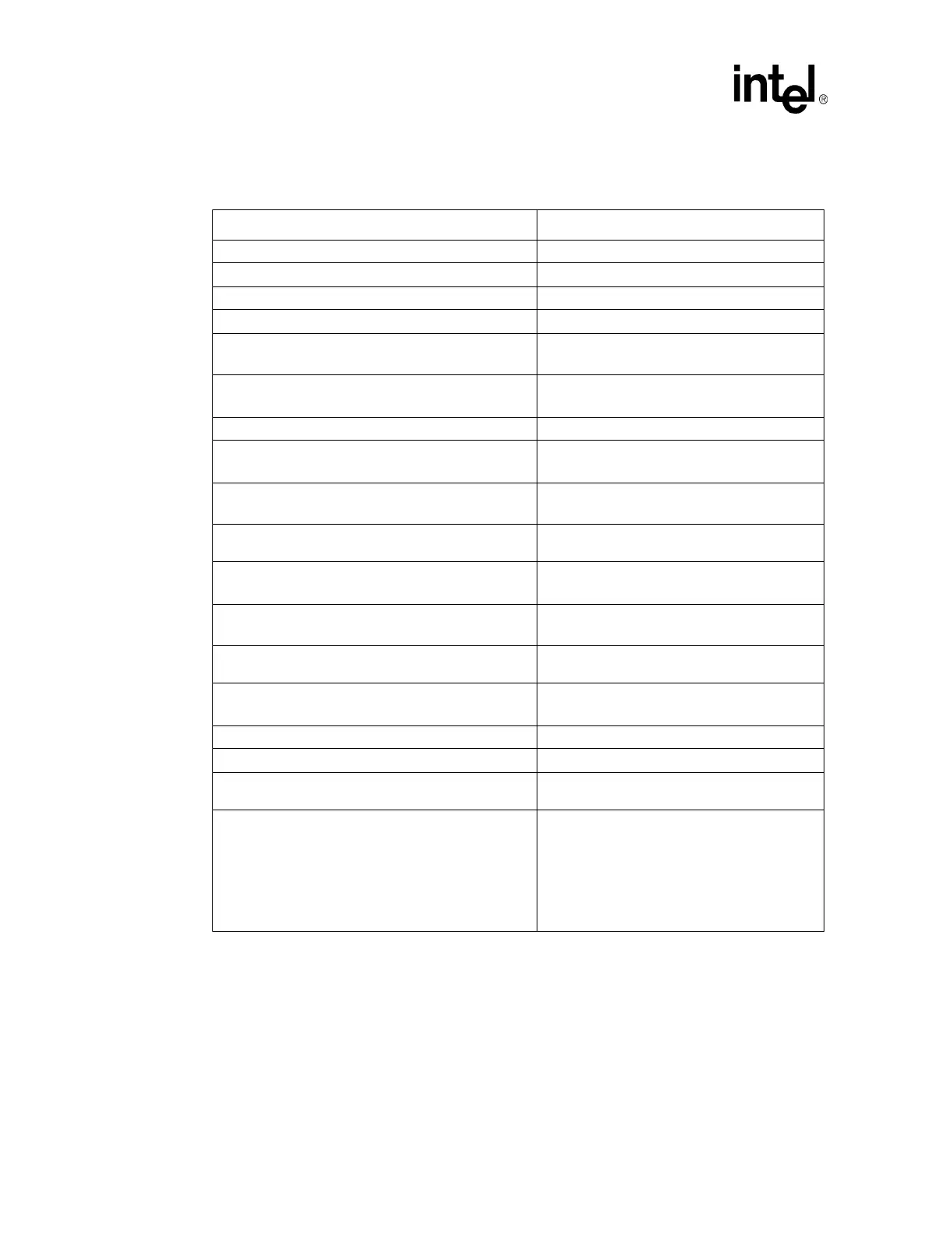
Table 32 presents the data signal group routing guidelines.
Table 32. Data Signal Group Routing Guidelines
Parameter Definition
Signal Group SDQ[71:0], SDQS[8:0], SDM[8:0]
Motherboard Topology Daisy Chain with Parallel Termination
Reference Plane Ground Referenced
Characteristic Trace Impedance (Zo) 55
Ω ±15%
Nominal Trace Width
Inner layers: 4 mils
Outer layers: 5 mils
Minimum Spacing to Trace Width Ratio
SDQ/SDM: 2:1 (e.g., 8 mil space to 4 mil trace)
SDQS: 3 to 1 (e.g., 12 mil space to 4 mil trace)
Minimum Isolation Spacing to non-DDR Signals 20 mils
Package Length P1
700 mils ± 300 mils
Refer to package length for details.
Trace Length P1+ L1 – GMCH Die-Pad to Series
Termination Resistor Pad
Min = 2”-L2
Max = 6”-L3-L2
Trace Length L2 – Series Termination Resistor Pad to
First DIMM Pad
Max = 0.75”
Total Length P1+ L1+L2 – Total Length from GMCH to
First DIMM Pad
Min = 2.0”
Max = 6”-L3
Trace Length L3 – First DIMM Pad to Last DIMM Pad
Min = 0.25”
Max = 2.0”
Trace Length L4 – Last DIMM Pad to Parallel
Termination Resistor Pad
Max = 1.0”
Total Length P1+ L1+L2+L3 – Total Length from GMCH
to Second DIMM Pad
Min = 2”+L3
Max = 6.0”
Series Termination Resistor (Rs) 10
Ω ±5%
Parallel Termination Resistor (Rt) 56
Ω ±5%
Maximum Recommended Motherboard Via Count Per
Signal
6
Length Matching Requirements
Match SDQS to SCK/SCK#
Refer to length matching Section 5.4.4.2 and
Figure 67.
SDQ/SDM to SDQS, to ± 25 mils, within each
byte lane.
Refer to length matching Section 5.4.4.3 and
Figure 68.
NOTES:
1. Power distribution vias from Rt to Vtt are not included in this count.
2. The overall minimum and maximum length to the DIMM must comply with clock length matching
requirements.