January 2007 275
Intel
®
855GME Chipset and Intel
®
6300ESB ICH Embedded Platform Design Guide
Schematic Checklist Summary
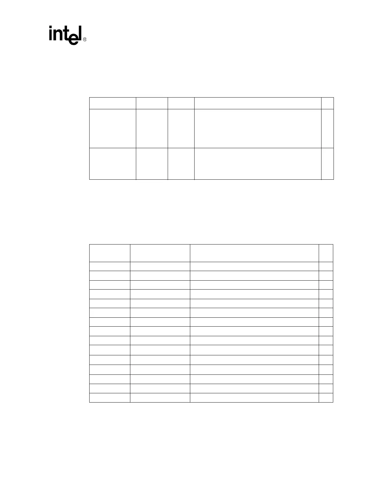
12.3.1.3 DIMM Decoupling Recommendation Checklist
Table 123 presents the DIMM decoupling recommendation checklist.
12.3.2 Frontside Bus (FSB) Checklist
Table 124 presents the FSB Checklist. Figure 151 depicts the Intel
®
855GME Chipset HXSWING
and HYSWING reference voltage generation circuit.
Table 123. DIMM Decoupling Recommendation Checklist
Pin Name F Qty Notes
√
V_1P25_MEMVTT
0.1 µF
4.7 µF
†
470 µF
(55
†
)
3
4
Place one 0.1 µF cap close to every two pull-up
resistors terminated to V_1P25_MEMVTT (VTT for
DDR signal termination). Place two 4.7 µF caps at either
end of the VTT island and one near the center. Four
470 µF capacitors may be placed as bulk decoupling.
Refer to Section 4.8.1.3 for more information.
V_2P5_SM
0.1 µF
100-150 µF
(220 µF
†
)
(100 µF
†
)
9 (15
†
)
4
(3
†
)
(1
†
)
A minimum of nine high frequency caps are
recommended to be placed between the DIMMS.
A minimum of four low frequency caps are required.
Refer to section Section 4.8.3.2 for more information.
† Used on Intel CRB.
Table 124. FSB Checklist (Sheet 1 of 2)
Pin Name
System
Pull-up/Pull-down
Notes
√
ADS# Connect directly to processor (ADS# signal).
HTRDY# Connect directly to processor (TRDY# signal).
DRDY# Connect directly to processor (DRDY# signal).
DEFER# Connect directly to processor (DEFER# signal).
HITM# Connect directly to processor (HITM# signal).
HIT# Connect directly to processor (HIT# signal).
HLOCK# Connect directly to processor (LOCK# signal).
BREQ0# Connect directly to processor (BR0# signal).
BNR# Connect directly to processor (BNR# signal).
BPRI#
Connect directly to processor (BPRI# signal).
DBSY#
Connect directly to processor (DBSY# signal).
RS[2:0]#
Connect directly to processor (RS[2:0]# signals).
HA[31:3]# Connect directly to processor (A[31:3]# signals).
HREQ[4:0]# Connect directly to processor (REQ[4:0]# signals).
HADSTB[1:0]# Connect directly to processor (ADSTB[1:0]# signals).