January 2007 315
Intel
®
855GME Chipset and Intel
®
6300ESB ICH Embedded Platform Design Guide
Layout Checklist
13.3.5 AC’97 Layout Checklist
13.3.5.1 RTC Layout Checklist
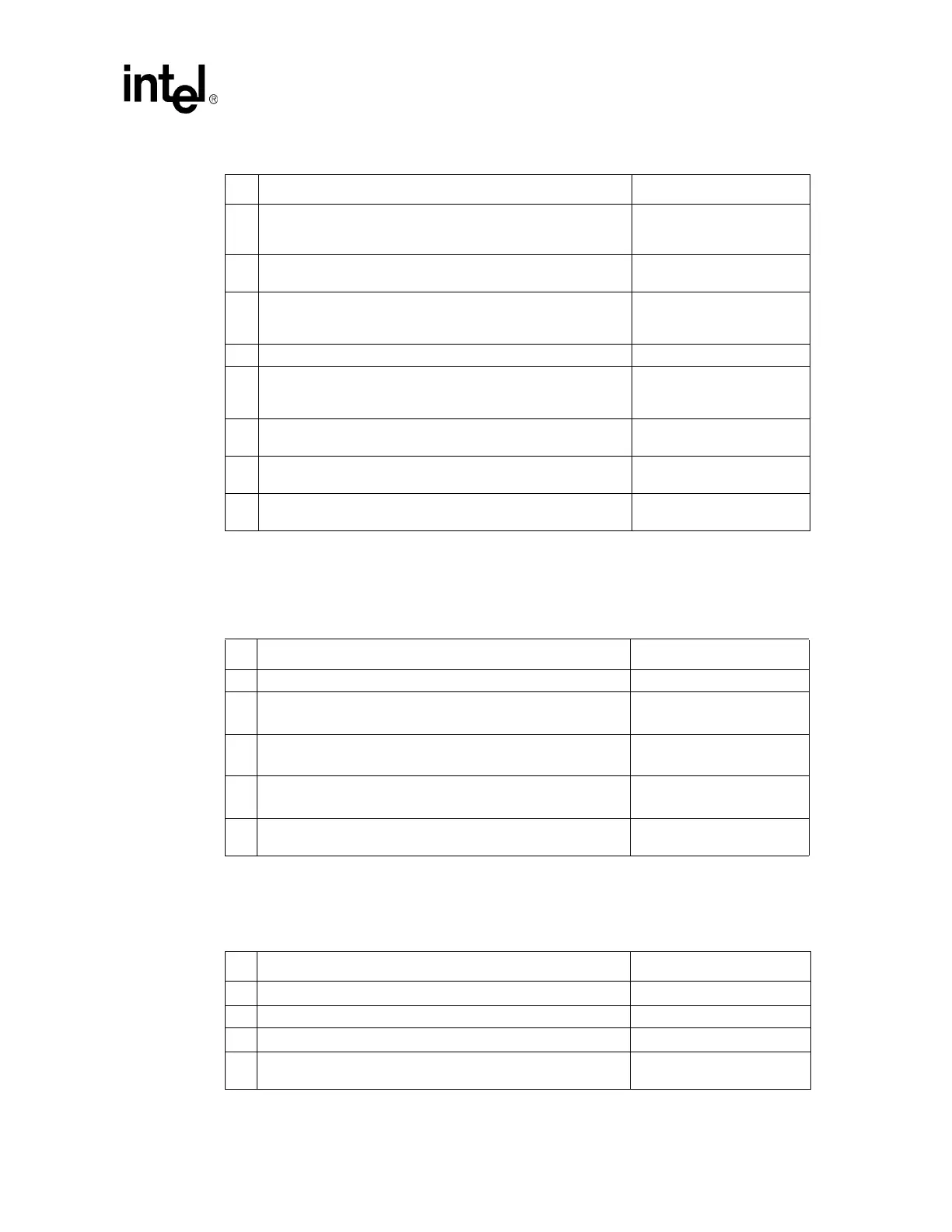
11
Minimize the length of high-speed clock and periodic signal traces
that run parallel to USB signal lines to minimize crosstalk. The
minimum recommended spacing to clock signals is 100 mils.
12
Use 45 mils minimum spacing between USB signal pairs and
other signal traces. This helps to prevent crosstalk.
13
USB signal pair traces should be trace length matched. Max trace
length mismatch between USB signal pair (such as DM1 and
DP1) should be no greater than 60 mils.
14 No termination resistors are needed for USB.
15
Short USBRBIAS and USBRBIAS# at the package, connect with
a 5 mils width, 5 mils spacing single trace 500 mils or less to the
22.6
Ω 1% resistor to ground.
16
Maximum length from the 6300ESB to the backpanel should not
exceed recommend length
17
Maximum length from the 6300ESB to the CNR should not
exceed recommend length
18
Maximum length from the 6300ESB to the Front Panel connector
should not exceed recommend length
Table 154. AC’97 Layout Checklist
# Layout Recommendations Comments
1 5 mils trace width, 10 mils spacing between traces.
2
AC_SDIN Max Trace Length
6300ESB to the Primary Codec or CNR connector is 14 inches
3
AC_SDOUT Max trace length
6300ESB to the Primary Codec or CNR connector is 14 inches
4
AC_BIT_CLK Max trace length
6300ESB to the Primary Codec or CNR connector is 14 inches
5
Series termination resistor on AC_BIT_CLK line should be no
more than 3.0 to 8.0 inches from the 6300ESB.
Table 155. RTC Layout Checklist
# Layout Recommendations Comments
1 RTC LEAD length = one inch maximum
2 Minimize capacitance between RTCX1 and RTCX2.
3 Put GND plane underneath Crystal components.
4
Don’t route switching signals under the external components
(unless on other side of board).
Table 153. USB 2.0 Layout Checklist (Sheet 2 of 2)
# Layout Recommendations Comments