January 2007 135
Intel
®
855GME Chipset and Intel
®
6300ESB ICH Embedded Platform Design Guide
System Memory Design Guidelines (DDR-SDRAM)
Length matching is not required from the DIMM1 to the parallel termination resistors. Figure 68
presents the length matching requirements between the SDQ, SDM, and SDQS signals within a
byte lane. Byte lane mapping is defined in Table 33.
5.4.4.4 SDQ to SDQS Mapping
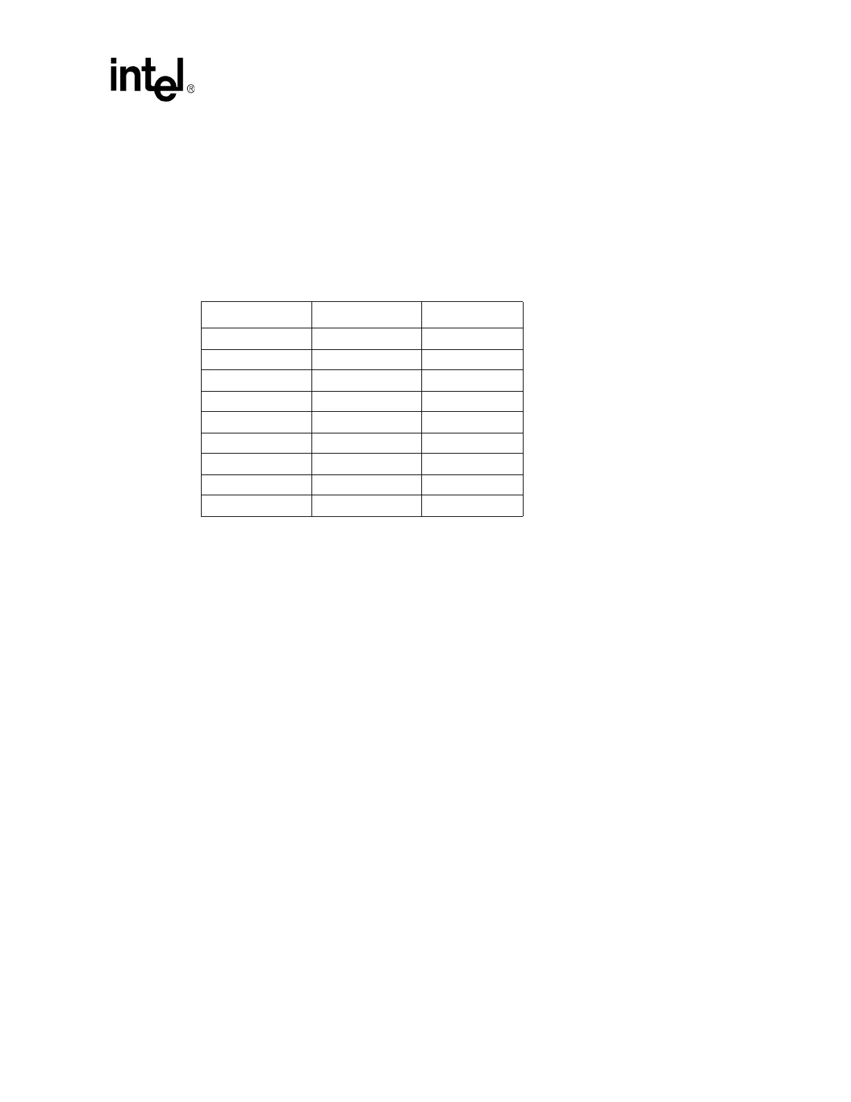
Table 33 defines the mapping between the nine byte lanes, nine mask bits, and the nine SDQS
signals, as required to do the required length matching.
Table 33. SDQ/SDM to SDQS Mapping
Signal Mask Relative To
SDQ[7:0] SDM[0] SDQS[0]
SDQ[15:8] SDM[1] SDQS[1]
SDQ[23:16] SDM[2] SDQS[2]
SDQ[31:24] SDM[3] SDQS[3]
SDQ[39:32] SDM[4] SDQS[4]
SDQ[47:40] SDM[5] SDQS[5]
SDQ[55:48] SDM[6] SDQS[6]
SDQ[63:56] SDM[7] SDQS[7]
SDQ[71:64] SDM[8] SDQS[8]