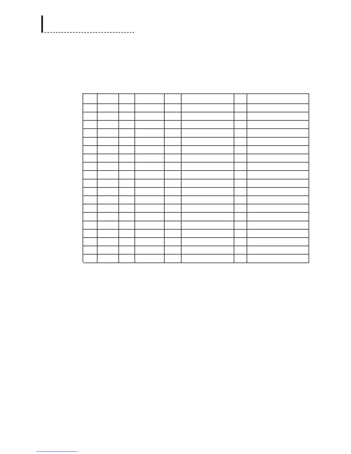
Microprocessor and Power Connector
The microprocessor access signals and the power signals are carried on a single 80-
pin connector, such as Samtec CLP-140-02-G-D-BE. The pin definitions are as per
the table, shown as if the connector was mounted on the component side. The
connector is mounted on the solder side of the board to minimize inter-connection
height. Therefore, the even and odd pins should be swapped.
1 +5V 2 +3.3V 41 A0 42 A1
3 +5V 4 +3.3V 43 A2 44 A3
5 +5V 6 +3.3V 45 A4 46 A5
7 -12V 8 +3.3V 47 A6 48 A7
9 -12V 10 GND 49 GND 50 GND
11 +12V 12 GND 51 INSTALLED 52 RD
13 +12V 14 GND 53 RESET 54 WR
15 GND 16 GND 55 IRQ 56 GND
17 GND 18 GND 57 GND 58 C27MHz
19 GND 20 GND 59 GND 60 GND
21 D0 22 D1 61 SDI_IN_256FS 62 SDI_IN_CH0
23 D2 24 D3 63 SPARE_3 64 SDI_IN_CH1
25 D4 26 D5 65 SDI_IN_BCLK 66 SDI_IN_CH2
27 D6 28 D7 67 SDI_IN_LRCLK 68 SDI_IN_CH3
29 GND 30 GND 69 GND 70 GND
31 D8 32 D9 71 SDI_OUT_BCLK 72 SDI_OUT_CH0
33 D10 34 D11 73 SDI_OUT_LRCLK 74 SDI_OUT_CH1
35 D12 36 D13 75 SPARE_2 76 SDI_OUT_CH2
37 D14 38 D15 77 SPARE_1 78 SDI_OUT_CH3
39 GND 40 GND 79 GND 80 GND
The timing waveforms for the protocol are shown in the diagram. The diagram
assumes that the address drivers and receivers are LVTH logic devices. The address
decoder CPLD device should be connected in parallel with the address drivers or
receivers. The system clock is 27MHz, and may not be delayed between the target
circuitry and the microprocessor clock. The maximum propagation delay of the
address decode device on the main card is 5nS. The chip select is programmed for
1w.s. (2 clock cycles). The read and write strobes are 1 clock wide. They are a
combinatorial function of the microprocessor CS, A, and RD/WR signals.
The target card generates CS signals as a combinatorial function of the address lines
only. The CS generator of the target card has a maximum output time of 10nS. For
read cycles, this allows a maximum device access time on the target board of 24nS.
For write cycles, the target should latch the data on the rising edge of C27 when WR
and the internally generated CS is valid. The WR signal should not be latched at the
interface, but should pass through to the target device. The device set-up time for
writes is 14nS.
92
DPS-475/575 Service Manual