2. Drive "FPGA_prog" active. Wait until "FPGA_init" and "FPGA_done" go active.
3. Drive "FPGA_prog" inactive. Wait until "FPGA_init" goes inactive.
4. Drive "FPGA_write" active.
5. Drive "FPGA_reset" active This enables the data write cycles for the FPGA
6. Write the bytes to the FPGA program portal. After every byte or group of bytes,
check that "FPGA_init" is still inactive. If "FPGA_init" is active, it indicates that
there is a programming error, or the data is corrupted.
7. Drive "FPGA_write" and "FPGA_reset" inactive.
8. Wait for "FPGA_done" to go active.
9. Pulse "FPGA_reset" active to bring the FPGA device into the operational state.
Wait for "Clock_OK" to become asserted prior to configuring any of the SPI
devices.
Note that "FPGA_init" is active low and "Clock_OK" and "FPGA_done" is active
high, as read at the microprocessor interface. "FPGA_prog", "FPGA_write", and
"FPGA_reset" are active high as written at the microprocessor interface.
CPLD Programming Connector
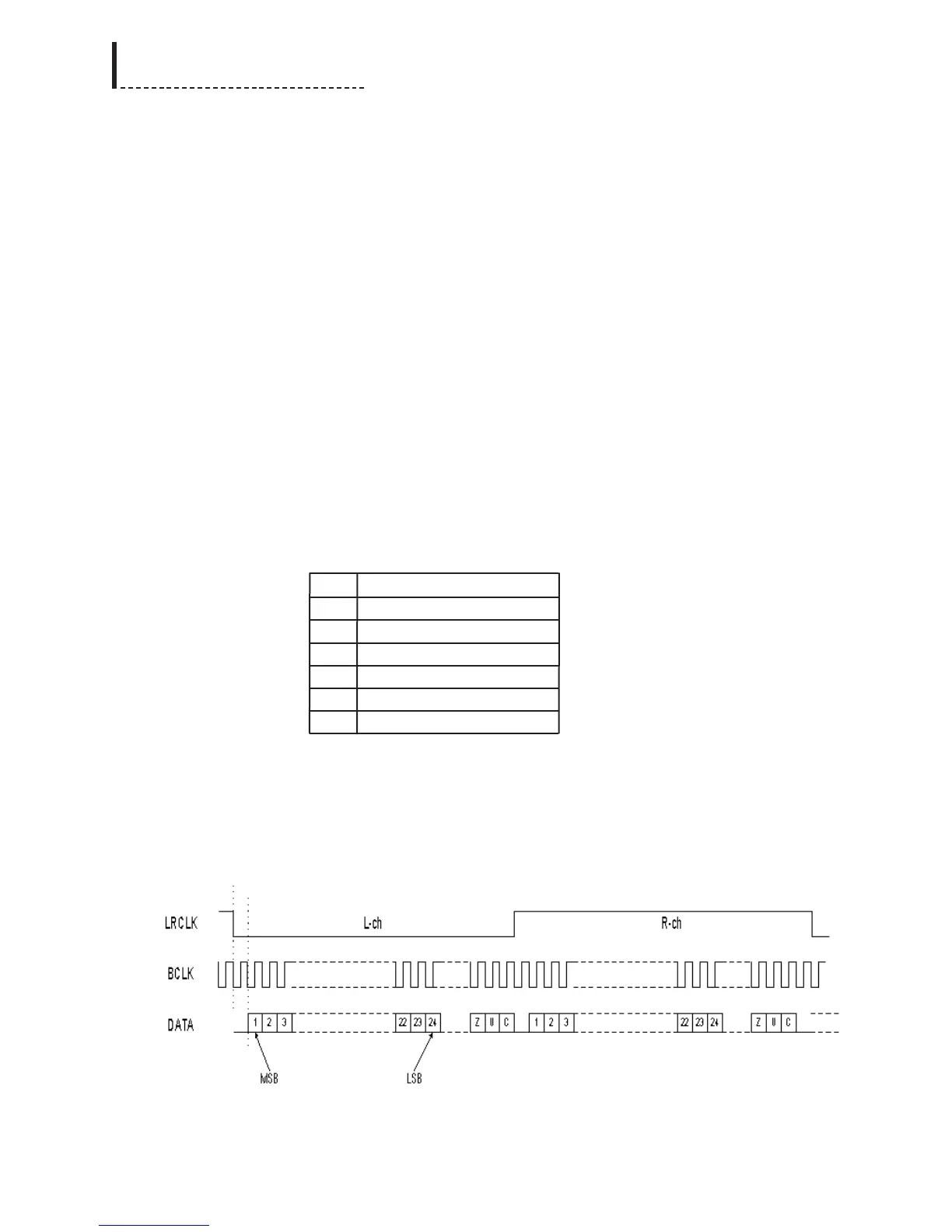
Pin # JTAG Program Interface
1 +5V
2 GND
3 TCK
4 TDC
5 TDI
6 TMS
The CPLD device is soldered to the PCB first then programmed using the JTAG
connector afterward.
I
2
S Data Format
The format for the audio serial protocol is 24-bit I
2
S, as per the diagram.
I
2
S Format for Serial Audio Bus
94
DPS-475/575 Service Manual