3.3.4 Test Register (M_CAN_TEST)
Write access to the Test Register has to be enabled by setting CCCR[TEST] to 1. All Test
Register functions are set to their reset values when CCCR[TEST] is reset.
Loopback mode and software control of M_CAN Tx are hardware test modes.
Programming of Tx other than 00 may disturb the message transfer on the CAN bus.
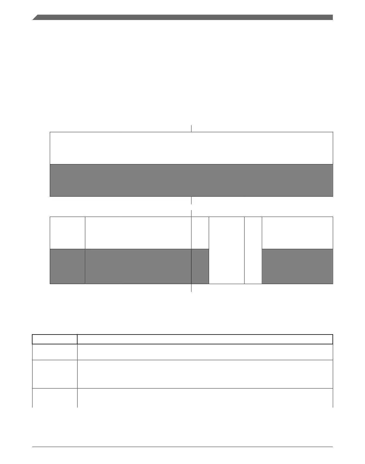
Address: 0h base + 10h offset = 10h
Bit 0 1 2 3 4 5 6 7 8 9 10 11 12 13 14 15
R
0
W
Reset
0 0 0 0 0 0 0 0 0 0 0 0 0 0 0 0
Bit
16 17 18 19 20 21 22 23 24 25 26 27 28 29 30 31
R
0 TDCV RX
TX
LBCK
0
W
Reset
0 0 0 0 0 0 0 0 u* 0 0 0 0 0 0 0
* Notes:
u = Unaffected by reset.•
M_CAN_TEST field descriptions
Field Description
0–17
Reserved
This field is reserved.
This read-only field is reserved and always has the value 0.
18–23
TDCV
Transceiver Delay Compensation Value
(0x00–0x3F)— Position of the secondary sample point, defined by the sum of the measured delay from
M_CAN Tx to M_CAN Rx and FBTP[TDCO]. Valid value are 0 to 63 M_CAN clock periods.
24
RX
Receive Pin
Monitors the actual value of M_CAN Rx
Table continues on the next page...
Memory Map and Register Description
MPC5777C Reference Manual Addendum, Rev. 1, 12/2015
32 Freescale Semiconductor, Inc.

 Loading...


